
Kingfordは「高品質、短納期、小量の試作生産から量産まで」というお客様のニーズにお応えします

DetaiLED explanation of parasitIC characteristics of circuit board via
PCB manufacturers, PCB designers and PCBA processors will explain the parasitic characteristics of PCB vias in detail.
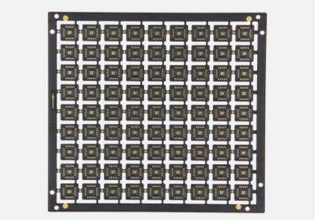
Via (via) is one of the important components of multilayer circuit boards, and the cost of drilling holes usually accounts for 30% to 40% of the cost of making circuit boards. In short, each hole on the circuit board can be called a through hole. Today, we will explain the parasitic characteristics of PCB via.
Parasitic characteristics of via are divided into parasitic capacitance and parasitic inductance:
1. Parasitic capacitance
The via itself has parasitic capacitance to the ground. If it is known that the diameter of the isolation hole of the via on the pavement is D2, the diameter of the via pad is D1, the thickness of the circuit board is T, and the dielectric constant of the board substrate is ε, Then the parasitic capacitance of the via is approximately C=1.41 ε TD1/(D2-D1)。 Parasitic capacitance of via will mainly affect the circuit by prolonging the rise time of the signal and reducing the speed of the circuit.
For example, for a circuit board with a thickness of 50Mil, if a via with an inner diameter of 10Mil and a pad diameter of 20Mil is used, and the distance between the pad and the ground copper area is 32Mil, we can approximately calculate the parasitic capacitance of the via through the above formula:
C=1.41 × four point four × zero point zero five zero × 0.020/(0.032-0.020)=0.517pF
The rise time variation caused by this part of capacitance is:
T10-90=2.2C(Z0/2)=2.2 × 0.517x(55/2)=31.28ps
It can be seen from these values that, although the effect of the rise delay caused by the parasitic capacitance of a single via is not obvious, the designer should carefully consider if the via is used for switching between layers for many times in routing.
2. Parasitic inductance
Parasitic capacitance and inductance exist in vias. In the design of high-speed digital circuits, the parasitic inductance of vias often brings more harm than the parasitic capacitance. Its parasitic series inductance will weaken the contribution of bypass capacitor and the filtering effectiveness of the whole power supply system. We can SIMply calculate the parasitic inductance of a via approximation using the following formula:
L=5.08h[ln(4h/d)+1]
Where L is the inductance of the via, h is the length of the via, and d is the diameter of the central drilling hole.
It can be seen from the formula that the diameter of the via has little influence on the inductance, while the length of the via has the greatest influence on the inductance. Using the above example, the inductance of the via can be calculated as:
L=5.08 × 0.050[ln(4 × 0.050/0.010)+1]=1.015nH
If the rise time of the signal is 1ns, the equivalent impedance is:
XL=πL/T10-90=3.19Ω
Such impedance cannot be ignored when there is high-frequency current passing through. In particular, the bypass capacitor needs to pass through two vias when connecting the power layer and the stratum, so the parasitic inductance of the vias will be multiplied. PCB manufacturers, PCB designers and PCBA processors will explain the parasitic characteristics of PCB vias in detail.


Telegram
Gerberファイル、BOMファイル、および設計ファイルをアップロードするだけで、KINGFORDチームは24時間以内に完全な見積もりを提供します。