
Kingfordは「高品質、短納期、小量の試作生産から量産まで」というお客様のニーズにお応えします

Check the assembly and design of the added layer PCB and FPC
The circuit board manufacturer, circuit board designer and PCBA manufacturer explain and check the relationship between the added layer circuit board and FPC assembly and design
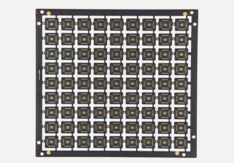
Because the signal line is configured along the X direction and Y direction. Therefore, bolt holes must be provided at the intersection of X and Y direction conductors so that the upper and lower lines can be connected. The bolt holes are arranged in a diagonal direction, whICh can be connected to the maximum number of bolt holes. In general, the density index of high-density circuit boards is expressed by the density of keyhole. The digital sample of keyhole that can be accommodated in each inch of square area is expressed in VPSG (Vias Per Square Grid) units. In addition to the fact that the plane circuit density of the laminated circuit board is three times that of the general FR4 printed circuit board, as the insulation layer thickness of the laminated circuit board is only 40um, it is also thinner than the FR4 circuit board, so the Z-direction density is twice that of the FR4 circuit board, so the circuit density of the entire laminated circuit board can be more than 10 times that of the general FR4 circuit board. As the line density of the laminated circuit board is still higher than that of the FR4 printed circuit board, if the precision required by the manufacturing process cannot be ensured, the production yield of the laminated circuit board will be greatly reduced.
The glass fiber substrate of the traditional FR4 printed circuit board is made by pressing the glass fiber cloth containing epoxy resin and copper foil. The mechanical drilling method is used to form the conductive holes between the upper and lower layers, and the photoetching method is used to form the lines. Therefore, part of the manufacturing process is mechanical processing, and part is chEMIcal processing.
In addition to a SMAll part of the perforation process, the laminated PCB is basically completed by the chemical process. Because the circuit density is still higher than that of the traditional FR4 circuit board, the traditional PCB inspection method cannot be used for quality control. And the control of process error is very important for the added layer circuit board, so how to select and control the process control parameters is a very important work. However, many process parameters cannot be directly inspected or observed, so how to monitor these process parameters is one of the key points to determine whether the mass production technology of the added layer circuit board is mature or not.
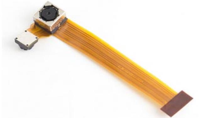
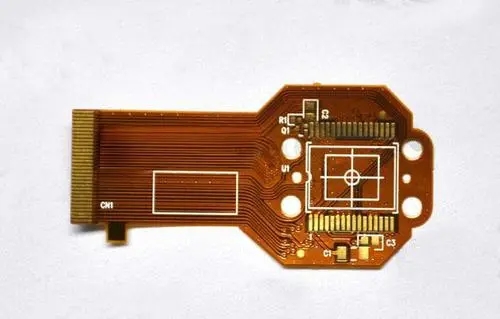
Relationship between FPC assembly and design
The general design principle of SMD pad for PCB can also be used for soft board, of course, the design method of soft board can also be modified according to needs. For the soft board, there are some design characteristics different from the hard board that deserve to be reviewed, especially some circuit design methods must pay special attention to avoid the risk of fracture. Obvious problems, such as the wrong direction of the line entering the welding pad, are a major problem.
Solder diffusion is another problem. If it happens, it may take many man hours to repair. The covering layer must have a sheltered area to prevent solder diffusion between terminals. Some producers use precision printing to supply appropriate solder paste for welding to prevent solder diffusion and obtain good welding.
Target design is also very important, which affects the precision of FPC fabrication and the convenience of assembly. The general target design will adopt circle, square, diamond, cross, etc. The design of each optical identification system must be subject to the equipment specifications adopted by the factory. Some identification systems are sensitive to the surface condition of the target, so properly maintaining the integrity of the surface treatment of the target is also helpful for target identification. For example, it is feasible to target through holes or gold-plated crosses. However, some problems may occur if the copper surface is used as the target, especially the copper surface is prone to oxidation and discoloration, which may lead to misjudgment of the identification system.
If electrical tests are required after assembly, these targets for electrical tests should also be considered in the design. The terminal size design of electrical test is very important, and proper design can reduce the error rate. Generally, the soft and hard board test points are not designed properly, which will affect the test results. The Circuit board manufacturer, circuit board designer and PCBA processor will explain and check the relationship between the added layer circuit board and FPC assembly and design.


Telegram
Gerberファイル、BOMファイル、および設計ファイルをアップロードするだけで、KINGFORDチームは24時間以内に完全な見積もりを提供します。