
Kingfordは「高品質、短納期、小量の試作生産から量産まで」というお客様のニーズにお応えします

Select High Frequency MICrowave RF PCB materials to Reduce RF circuits
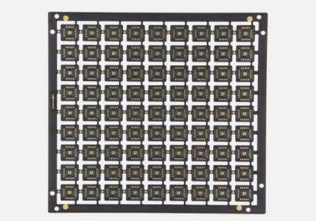
PCB manufacturing, PCB design and PCBA processing manufacturers explain how to select high-frequency microwave RF PCB materials to reduce the size of RF circuits
With the increasing demand for the mobility and portability of electronic equipment, the miniaturization of high-frequency microwave and RF circuit design becomes more and more important. Before starting to design electronic products, selecting an appropriate high-frequency microwave RF circuit board material will help to design SMAller RF and microwave circuits. For a given frequency range, using high-frequency PCB materials with higher dielectric constant (Dk) will generally reduce the design size and structure of the circuit. However, using boards with higher Dk values will increase the insertion loss of the circuit, and may also reduce the performance of other aspects of the circuit. At the same time, the Dk value of the PCB material will also affect the index parameters of the circuit, such as radiation loss, dispersion, coupling, etc.
For a given frequency, the wavelength in the medium will decrease with the increase of the circuit board material Dk, resulting in a smaller circuit size designed on the circuit board material with a higher Dk value than on the high-frequency microwave RF circuit board material with a lower Dk value. In addition, high frequency microwave RF circuit board materials with high Dk value will also reduce the phase velocity of electromagnetic wave (EM) passing through these materials. Dk of high frequency microwave RF circuit board materials is usually measured through the z-axis direction (i.e. thickness direction) of the material at 10GHz. The z-axis Dk value of commercial PCB materials can be as high as 10 (or higher) or as low as 2 (compared with Dk of air equal to 1). However, objectively speaking, if the Dk value is 6 or higher, it can be considered as a plate with high dielectric constant.
The transmission line made of high-frequency microwave RF circuit board material with low Dk value has faster phase velocity. For the miniaturization design of phase sensitive circuits (such as phased array antenna), the influence of Dk must be considered. In addition, the high frequency microwave RF PCB materials with higher Dk values show greater dispersion than those with lower Dk values. High frequency microwave RF circuit board materials with high Dk values are usually used for directional couplers and other circuits requiring high coupling coefficients.
As far as Dk is concerned, high frequency microwave RF circuit board materials are usually anisotropic. Although Dk values of materials in the three axes are different, people usually compare each other according to Dk values of materials in the z-axis direction. For materials with higher Dk values, the Dk difference between the z-axis and x-y plane of the circuit is often greater than that of materials with lower Dk values. The Dk values in all three dimensions of the high frequency microwave RF circuit board material will jointly determine the performance of the transmission lines (such as microstrip lines) made on the material. For many high frequency circuits, it is usually unnecessary to consider the anisotropy of the high frequency microwave RF circuit board material Dk, but the anisotropy does bring some potential unknown problems, especially when the Dk value on the x-y plane is very different from the Dk value on the z axis. This difference may cause unexpected problems for edge parallel coupLED circuits, because their coupling is highly dependent on the Dk value on the x-y plane.
When trying to miniaturize the circuit, the easiest way to think of is to minimize the thickness of the high-frequency microwave and RF circuit board material, but the thickness of the high-frequency microwave and RF circuit board material will affect the performance of many indicators of the high-frequency circuit. Although the radiation loss of high-frequency circuit will increase with the increase of frequency, thicker PCB materials will also show higher radiation loss than thinner PCB materials with the same Dk value. For a given circuit layout and design, the selection of Dk also affects the size of radiation loss, because the radiation loss of PCB materials with higher Dk value is lower than that of PCB materials with lower Dk value.
For circuits that may cause resonance or stray interference (for example, between circuits in high frequency microwave RF of multilayer PCB), it is beneficial to use thinner PCB materials. The degree of resonance spurious usually depends on the type of transmission lines in the circuit. For example, microstrip transmission lines are more vulnerable to resonance and propagation problems than other types of RF/microwave transmission lines (such as striplines, CPW transmission lines of coplanar waveguides). Thinner PCB materials can help reduce the volume of PCB high-frequency microwave RF boards, while limiting radiation loss and transmission line propagation problems, such as resonance and intermodulation. The common engineering experience is to use high-frequency microwave RF PCB materials thinner than the quarter wavelength of the highest working frequency of the circuit. But the safer way is to choose a high-frequency microwave RF PCB material thinner than the eighth wavelength of the highest working frequency in thickness.
The line width size of transmission lines (such as microstrip lines) will depend on the thickness of high-frequency microwave RF circuit board materials (such as circuit laminates or prepreg materials). The circuit using a thicker substrate will widen the conductor width, which can reduce the conductor loss and insertion loss of the circuit. However, in this case, some electromagnetic wave propagation problems may occur. In order to select the thickness of PCB material suitable for high frequency design, the conductor width should generally be less than one eighth of the wavelength of the highest operating frequency.
The Dk of the high frequency microwave RF circuit board material plays an important role in determining the transmission line conductor width, because the same size conductor designed on the high Dk high frequency microwave RF circuit board material has lower impedance than the same circuit on the low Dk material. Therefore, in order to maintain the 50 Ω characteristic impedance of the circuit, the circuit designed on the PCB material with higher Dk value will be narrower.
A wise choice
Many tradeoffs need to be considered when designing circuits using high frequency microwave RF PCB materials with different Dk values. Using high Dk high frequency microwave RF circuit board materials can not only reduce the circuit size, but also achieve high-performance miniaturized circuits by combining high Dk and low Dk circuit board materials. For example, the size and height of a band-pass filter composed of resonant cells depend on the Dk of the PCB material. Because the spacing between each filter unit determines the coupling strength in the circuit affected by the circuit board material Dk. High frequency microwave RF circuit board materials with high Dk provide stronger coupling, and allow more space between filter resonance units.
In order to verify the advantages of using high frequency microwave RF circuit board materials with different Dk values (combining materials with different Dk values into a composite component), a band-pass filter is designed on the composite materials of high Dk and low Dk high-frequency microwave RF circuit boards. The high Dk material used in this filter is RT/duroid ® The Dk value of 6010.2LM line laminate is 10.7; The low Dk materials used for and are 2929 prepreg, with a Dk value of 2.9. Both materials are from Rogers. Because the high frequency microwave and RF circuit board materials with different Dk values will bring differences to the circuit performance, it is necessary to carry out SIMulation with the help of computers, and determine the required proportion of the thickness of two different materials through modeling. This modeling method can help us design a perfect composite filter. The experimental results show that the size of the filter designed by composite materials not only maintains the size of a single high Dk material, but also has improved electrical performance. For example, the high order harmonic resonance is significantly reduced, and the stopband characteristics of the filter are also significantly improved. Research shows that by using more than one PCB material in the circuit, it is often possible to miniaturize the circuit without sacrificing performance. PCB manufacturers, PCB designers and PCBA manufacturers explain how to select high-frequency microwave RF PCB materials to reduce the size of RF circuits.


Telegram
Gerberファイル、BOMファイル、および設計ファイルをアップロードするだけで、KINGFORDチームは24時間以内に完全な見積もりを提供します。