
Kingfordは「高品質、短納期、小量の試作生産から量産まで」というお客様のニーズにお応えします

What is the meaning of PCBA processing stamp holes?
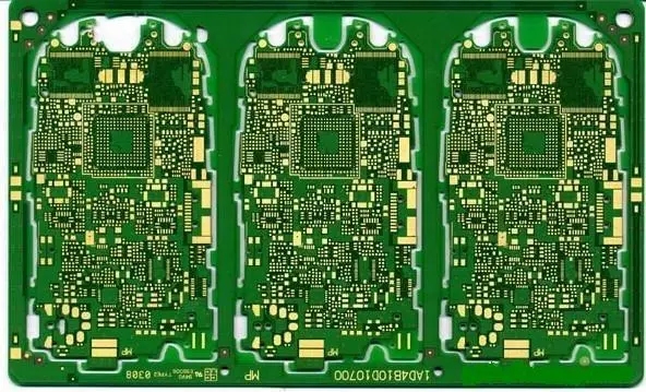
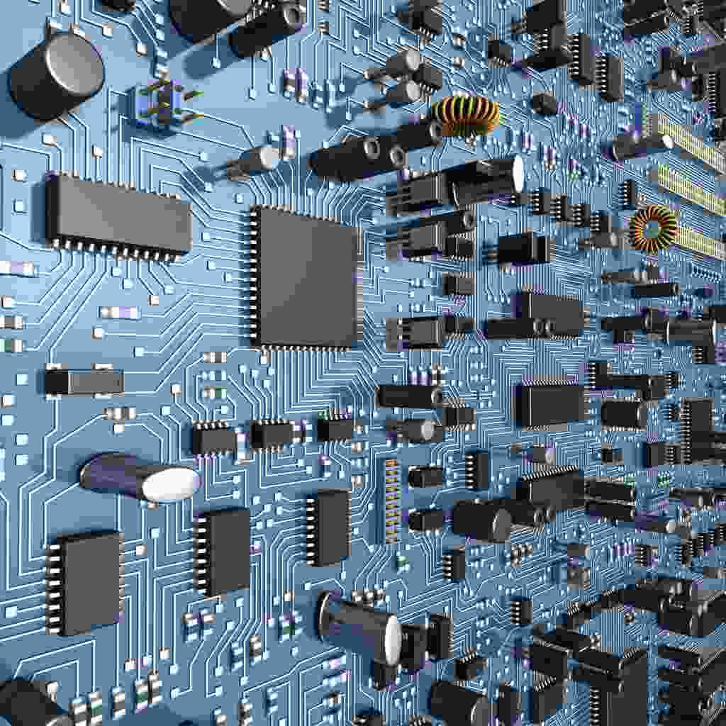
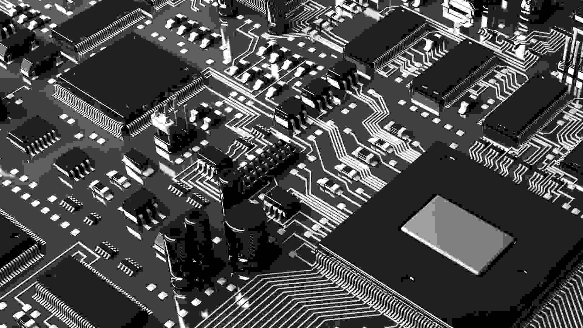
PCBA processing is to connect various electronIC components on PCB board through surface mount (SMT), plug-in (DIP) and other electronIC assemblies. PCBA process flow mainly includes SMT, AOI, DIP, FCT testing and other processes. Due to the size difference of electronic components, there will be different processes and requirements in assembly and insertion. The assembly density of PCBA is relatively high, and the SMAll size and light weight of electronic products also have certain changes and requirements in mounting. The reliability, seismic resistance and excellent weldability of the products have high requirements for the hardware and software facilities of PCBA processing.
The stamp hole during PCBA processing refers to the inside of the main board interface splicing mode. The small board and the middle of the small board must be connected with each other to facilitate laser cutting. There will be some small round holes on the ribs, SIMilar to the holes on the edge of commemorative stamps, which are calLED stamp holes.
The hole shape of the stamp is close to the round hole design scheme cut in commemorative stamps. Its advantage is that the compressive strength is better than V-Cut, and unlike Tap, which has to be cut by Router machines and equipment, it can break immediately. However, the defect is that the fracture surface is not easy to control accurately. If the distance between the lines is too close, it is very easy to cause damage to the lines, which in turn leads to the filing of fees.
In general, the PCB assembly method can be used for stamp hole technicality or double corresponding V-shaped groove cutting technicality. When selecting stamp holes, it should be noted that the stained edges should be evenly distributed around each piece of PCB assembly method to prevent deformation due to uneven PCB support during electric welding. The part of stamp hole shall be close to the inner side of PCB board to prevent the residual burrs at stamp hole from harming the whole equipment assembly line of customers after separation by panel assembly. When selecting V-shaped grooves on both sides, the deep layer of the V-shaped groove should be controlled at 1/3 of the top and bottom (the sum of grooves on both sides). It is specified that the groove specification is accurate and the deep layer is symmetrical.
PCB manufacturers, PCB designers and PCBA processors will explain to you what the stamp holes in PCBA processing mean.


Telegram
Gerberファイル、BOMファイル、および設計ファイルをアップロードするだけで、KINGFORDチームは24時間以内に完全な見積もりを提供します。