
Kingfordは「高品質、短納期、小量の試作生産から量産まで」というお客様のニーズにお応えします


8 Principles and 15 Precautions for PCBA Processing
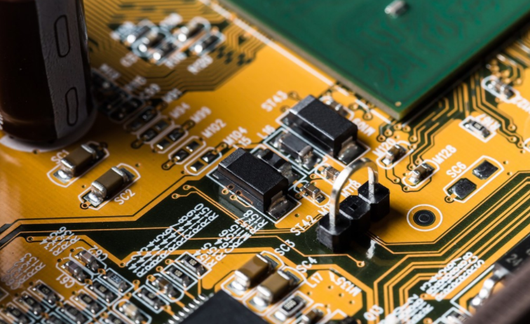
1 Preferred crimp and PCBs surface mount components
Surface mounted parts and crimping parts have good processability.
With the development of component packaging technology, most components can be purchased according to the package category suitable for reflow, including plug-in components that can be reflowed through holes. If the design can realize full surface installation, the installation effICiency and quality will be greatly improved.
Crimping components are mainly multi pin connectors. This packaging also has good manufacturability and connection reliability, which is also the preferred category.
2 and consider the packing ratio and pin spacing as a whole
Package size and pin spacing are the most important factors affecting the whole PCB process. On the prEMIse of selecting surface mount components, a group of packages with SIMilar or appropriate technical performance shall be selected, and a certain thickness of stencil printing shall be pasted onto a PCB with a specific size and installation density. For example, for mobile phone boards, the selected packaging is suitable for printing with 0.1mm thick stencil solder paste.
3. Shorten process path
The shorter the process route, the higher the production efficiency and the more reliable the quality. The optimized design of the process route is as follows:
Single side reflow welding;
Double side reflow welding;
Double side reflow+wave soldering;
Double side reflow+selective wave soldering;
Double side reflow welding+manual welding.
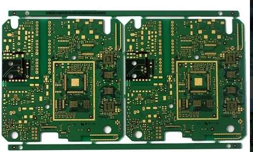
Circuit board

4. Optimize component design
The layout design of main components mainly involves the layout direction and spacing Layout of components. The arrangement of components must meet the requirements of welding process. Scientific and reasonable design can reduce the use of incorrect welding tools and joints, and optimize the design of steel mesh.
5. Consider the design of welding pad, welding resistance and steel mesh window
The design of pad, solder mask and mold window determines the actual distribution of solder paste and the formation process of solder joint. It is very important to coordinate the design of welding pad, welding resistance and steel mesh to improve the welding speed.
6. Focus on new packaging
The so-calLED new software packages do not completely refer to the new software packages on the MARKet, but your own company has no experience in using these software packages. For the import of new packaging, SMAll batch verification must be carried out. Other people can use it, but that doesn't mean it can also be used. On the premise of using it, you should understand the characteristics of the process and the scope of problems, and master the countermeasures.
7. Focus on BGA, chip capacitors and crystal oscillators
BGA, chip capacitor and crystal oscillator are typical stress sensitive components. PCB bending and deformation shall be avoided as far as possible in welding, assembly, workshop rotation, transportation, use and other links.
8. Study cases to improve design standards
Manufacturing design rules are derived from production practices. It is very important to optimize and improve the design rules according to the continuous occurrence of poor assembly or faults for improving the design for manufacturability.
When designing PCB boards, engineers must reduce costs and improve assembly quality on the premise of meeting the requirements of overall electromechanical efficiency, mechanical structure and reliability. So, what problems should be paid attention to in the design for manufacturability of PCB? Share 15 attention questions.
1. Minimize the number of PCB layers. Single panel can be used to replace double-sided board, or double-sided board can be used to replace Multilayer board, so as to reduce PCB processing cost as much as possible.
2. Try to use reflow soldering process, because reflow soldering has more advantages than wave soldering.
3. PCB assembly process shall be minimized and no clean process shall be adopted as far as possible.
4. Whether the requirements of SMT process and equipment on PCB design are met.
5. Whether the shape and size of PCB are correct, and whether the splicing process is considered for small size PCB.
6. Check whether the edge clamping design and locating hole design are correct.
7. Whether the locating hole and non grounding mounting hole are marked as non-metallic.
8. Whether the marking pattern and its position meet the requirements, and whether 1~1.5mm is reserved around the solder mask.
9. Have you considered the requirements of environmental protection?
10. Whether the selection of base materials, components and packaging meets the requirements.
11. Whether PCB pad structure (shape, size, spacing) meets the DFM specification
12. Whether the width, shape, spacing of the lead wire and the connection between the lead wire and the pad meet the requirements.
13. Whether the general layout of components and the minimum spacing between components meet the requirements; Whether the rework size is considered around large parts and whether the polarity arrangement direction of parts is as consistent as possible.
14. Whether the hole diameter and pad design of 挿 parts conform to DFM specification; Whether the distance between adjacent parts is favorable for manual operation.
15. Whether the solder mask and screen pattern are correct, and whether the component polarity and IC pin are marked.


Telegram
Gerberファイル、BOMファイル、および設計ファイルをアップロードするだけで、KINGFORDチームは24時間以内に完全な見積もりを提供します。