
Kingfordは「高品質、短納期、小量の試作生産から量産まで」というお客様のニーズにお応えします

Processing and assembly of double-sided PCB and PCBA
Due to the increasingly high functional requirements of products, ordinary single panel can no longer meet the needs of functionality At this historICal moment, the double-sided printed PCB circuit board appeared This means that there are wires on both sides of the circuit board It is usually made of epoxy glass cloth copper clad plate It is used in the field of communication electronic equipment, advanced instruments, high-performance electronic computers, etc The typical process for manufacturing double-sided plated-hole printed boards is the bare copper-clad solder mask process (SMOBC). The process is as follows:
Blanking of double-sided copper clad plate - CNC drilling inspection, deburring, brush chEMIcal plating (through hole metallization) - (full plate electroplating of thin copper) - inspection and cleaning of negative circuit pattern of screen printing, Curing (dry film or wet film, exposure, development) - checking and repairing circuit pattern electrotinning (anti-corrosion nickel/gold) - removing printed materials (photosensitive film) - etching copper - (removing tin) and cleaning and brushing a layer of hot curing green oil silk screen to print solder mask pattern (photosensitive dry film or wet film, exposure, development, thermal curing, ordinary photosensitive heat) curing and oil recording Curing - (tin spraying or organic solder mask) - shape treatment, cleaning, drying, power switch test, packaging inspection, finished product delivery.
Assembly of finished products PCBA processed products
1. Prepare materials, equipment and tools required for Circuit board assembly
1. A DC regulated power supply and a multimeter;
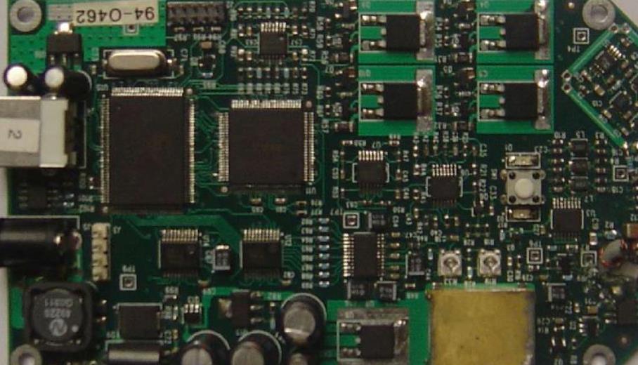
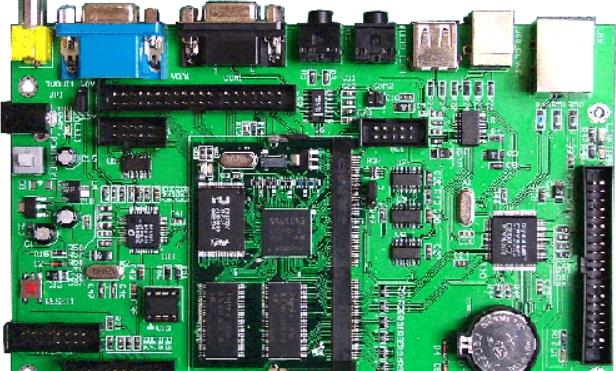
2. Soldered circuit board;
Circuit board

3. List of kits and enclosures of products to be assembLED, as well as relevant accessories of the machine;
4. Electric screwdriver, rag, electronic label (product identification code);
2. Inspection before assembly
1. Detailed inspection of the list to be assembled and circuit board inspection
2. Check the product shell
3. Check the housing of the product kit for defects and damage.
4. Check the printed board. Visually check whether the printed board is in good condition, whether the surface solder coating is in good condition, and whether there are obvious short circuit and short circuit defects. Use a multimeter to check whether there is a short circuit between the power supply and the grounding on the printed board.
3. Final assembly and delivery
1. The boards with BGA and IC shall use heat dissipation adhesive and crash pad;
2. Align the printed boards and place them in the housing. Align the screw hole, pay attention not to collide the floating resistor and other parts with the housing;
3. Install the screws fixing the printed circuit board, cover the housing, and tighten the assembly screws;
4. Check the appearance for damage and other appearance defects;
5. Attach product labels;
6. Transfer to the back end, such as aging test;
The whole PCBA assembly process is roughly as follows If there are special process requirements, they can be improved according to the relevant technical requirements of DFM
The above is the explanation given by the editor of PCB circuit board company.
If you want to know more about PCBA, you can go to our company's home page to learn about it.
In addition, our company also sells various circuit boards,
High Frequency Circuit Board and SMT chip are waiting for your presence again.


Telegram
Gerberファイル、BOMファイル、および設計ファイルをアップロードするだけで、KINGFORDチームは24時間以内に完全な見積もりを提供します。