
Kingfordは「高品質、短納期、小量の試作生産から量産まで」というお客様のニーズにお応えします

PCB manufacturers explain DIP packaging and process flow in detail
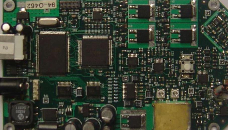
1、 DIP package is also calLED DIP package or DIP package (DIP or DIL for short), whICh is a packaging method of integrated circuit. The shape of integrated circuit is rectangular, and there are two parallel rows of metal pins on both sides of the integrated circuit, which are called pins. components packaged in DIP can be soldered into electroplated through-hole of printed circuit board or inserted into DIP socket. Because some new components only provide products packaged with Surface Mount Technology, many companies produce adapters that convert SMT components into DIP packaging,
1、 DIP encapsulation
dual in line package (in English: dual in line package) is also called DIP package or DIP package (DIP or DIL for short), which is a packaging method of integrated circuit. The shape of integrated circuit is rectangular, and there are two rows of parallel metal pins on both sides of the integrated circuit, which are called array pins. Components packaged in DIP can be soldered into electroplated through-hole of printed circuit board or inserted into DIP socket.
Because some new components only provide products packaged by surface mount technology, many companies produce adapters that convert SMT components into DIP packaging. ICs packaged by surface mount technology can be placed in adapters, and then connected to bread boards or other circuit prototypes (like hole boards) matching in-line components like DIP packaging components.
The package of dual in-line package chip is generally made of plastic or ceramic. Ceramic packaging has good air tightness and is often used in equipment requiring high reliability. However, most dual in-line package chips use thermosetting resin plastic. A curing cycle of less than 2 minutes can produce hundreds of chips.
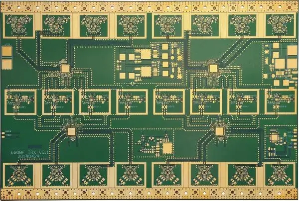
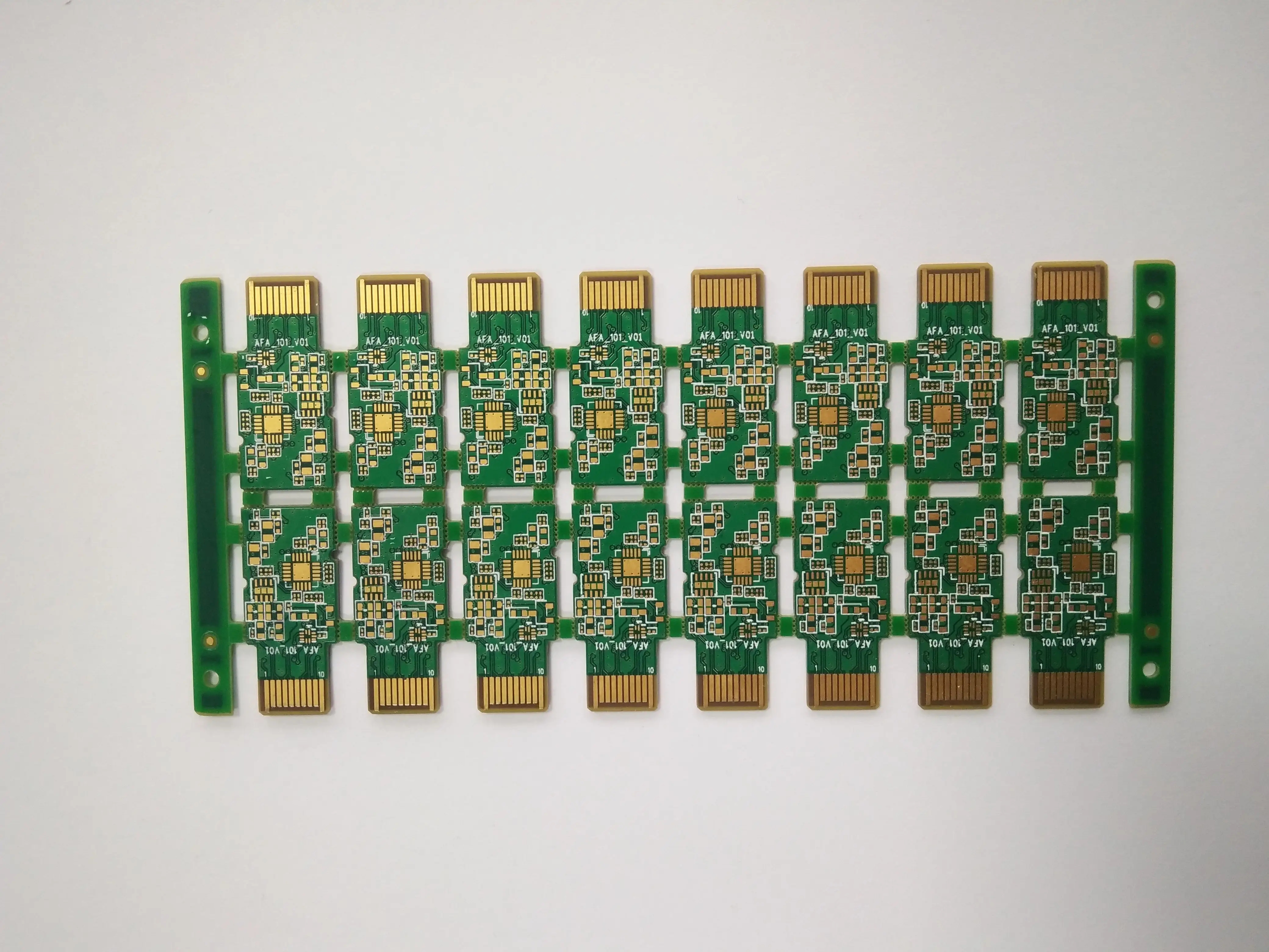
2、 DIP plug-in process flow
The DIP plug-in processing process is a part of the whole PCBA processing process. It refers to the manual plug-in processing of large electronIC components that cannot be put into chip processing. After wave soldering processing and other processes, the finished PCBA processing products are finally formed. The process of DIP plug-in processing is difficult, and professional technical guidance personnel are required for processing guidance. Generally speaking, its technological process can be divided into three steps: arranging process, wave soldering and quality inspection. Next, we will explain the processing steps of each process in detail.
1. Operation scheduling
The operator determines the item number and direction of the material according to the BOM list, and arranges each person on the DIP plug-in cable to assign components to each employee. At this time, the first sample needs to be confirmed. The last employee conducts inspection, compares inspection with the BOM one by one, and then submits it to the personnel of the Quality Department to check the first piece.
2. Wave soldering
After the confirmation of the first piece, carry out batch production, and then conduct wave soldering to fix the electronic components on the PCB. Wave soldering is divided into lead soldering and lead-free soldering. It depends on the customer's requirements and the size of electronic components to decide whether to perform lead soldering or lead-free soldering. During wave soldering, adjust and control the speed of wave soldering chain, the height of tin spraying and wave soldering, and the most important processing time, which is generally 2-3 seconds. At the same time, some electronic components with strong thermal sensitivity shall be manually welded. Of course, it is also necessary to cut the feet of the materials after welding.
3. Quality Inspection Department
The inspection of the Quality Department is an important process to ensure the quality of PCB boards. It should inspect whether there is solder, whether there is faulty soldering, floating height, etc., and carry out fine inspection according to the international standard IPC6101 to assist customers in their requirements to ensure the delivery of products that customers are satisfied with.


Telegram
Gerberファイル、BOMファイル、および設計ファイルをアップロードするだけで、KINGFORDチームは24時間以内に完全な見積もりを提供します。