
Kingfordは「高品質、短納期、小量の試作生産から量産まで」というお客様のニーズにお応えします

Wet and PCB board surface treatment
Abrasive Abrasive, brush
Various materials are used to pre clean PCB board surface and brush copper surface, such as polymer non-woven fabrIC, non-woven fabric mixed with carborundum, or various types of sandless materials, and pumice powder (Pumice Slurry), etc This is calLED abrasive However, the power of this brush material mixed with sand is usually implanted on the copper surface, resulting in problems of adhesion and solderability of the subsequent photoresist or electrodeposit The attached figure is a schematic diagram of brush material fiber mixed with sand particles
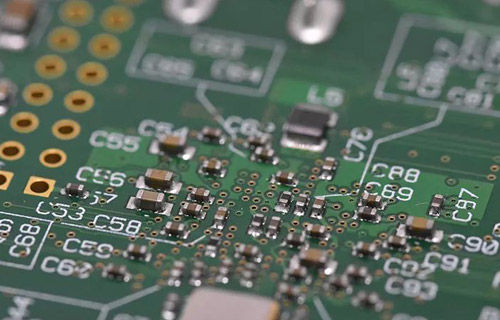
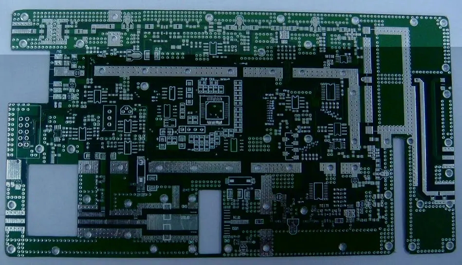
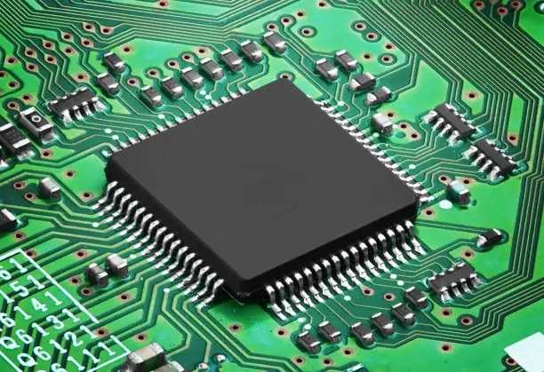
PCB board

2. Air knife
At the outlet of devices on various process lines, there is often a knife edge blowing air knife with high-temperature and high-pressure air, which can quickly dry the board surface, facilitate handling and reduce oxidation opportunities.
3. Defoamer
In the PCB manufacturing process, such as the cleaning process of dry film developer, a large amount of foam is generated due to the dissolution of a large amount of organic film data, and air is mixed in the selection and spraying process, which is very inconvenient for the process. It is necessary to add chEMIcals to reduce the surface tension in the plating solution, such as octanol or organic silicon as defoamer, to reduce the trouble of on-site operation. However, silicon resins containing cationic interface active agents of silica compounds are not suitable for metal surface treatment. Because it is not easy to clean after contacting the copper surface, the subsequent coating has poor adhesion or poor weldability.
4. Cohesive tack coat
Subsequent layer: refers to the surface to be bonded (or bonded), which must be kept clean to achieve and maintain good bonding strength. It is called "bonding".
5. Bank Agent
It refers to the organic additives added in the etching solution so that they can play a role in the film adhesion on both sides of the line with weak water flow, thus weakening the attack of the agent and reducing the degree of lateral erosion (Cmdercut). It is an important condition for fine line etching. The agent is mainly a secret of the supplier.
6. Bright DIP treatment
It is a slight bite on the metal surface to make it look smoother and brighter. The wet treatment of water bath is called.
7. Chemical grinding
It uses chemical wet method to conduct corrosion treatment on metal materials to varying degrees, such as surface roughening, deep etching or application of precise special resistance, and then selective etching, to replace some mechanical processing methods of stamping operation, also known as chemical blanking or photochemical processing (PCM) technology, which not only saves expensive mold costs and preparation time, but also eliminates the trouble of residual stress.
8. Coating, film, surface layer
Usually refers to the treatment layer made on the surface of the sheet. Broadly speaking, it refers to any surface treatment layer.
9. Conversion film
It refers to some metal surfaces, which can be converted into a compound protective layer on the surface only by soaking in a specific tank. For example, phOSPhating treatment of iron surface, chromating treatment of zinc surface or zinc treatment of aluminum surface can be used as "primer" (punching) of subsequent surface treatment layer. It also has the function of increasing adhesion and enhancing corrosion resistance.
10. Degrease
Traditionally, it refers to the need to remove a large number of oil stains left by machining before electroplating metal objects. Generally, the "vapor degreasing" method of organic solvent or the immersion degreasing method of emulsion solution are often used. However, it is not necessary to degrease during the processing of the circuit board because there is almost no contact with oil during all processing, which is different from metal electroplating. However, the pretreatment of paperboard still needs to use "cleaning" treatment, which is not exactly the same as degreasing in concept.
Etching factor
In addition to the downward etching of the front side of the copper etching, the etching solution will also attack the unprotected copper surface on both sides of the line, called undercut, resulting in mushroom shaped etching defects. Etching factor is the quota of etching quality. The term etching factor used in the United States (mainly IPC) is completely contrary to the European interpretation. Americans say that it is "the ratio of positive etching depth to side etching concavity", so Americans say that the greater the "etching coefficient", the better the quality; The European definition is just the opposite, but the SMAller the "factor", the better the quality. That's good. It's easy to make mistakes. However, over the years, the achievements of IPC in circuit board aCADemic activities and publications have been in a leading position in the world industry. The definition of IPC can be regarded as a standard cost, and no one can replace it.
Etchant Etchant
In the circuit board industry, it refers to the chemical bath used for etching copper layers. At present, acidic copper chloride solution has been used for inner laminates or single panels, which has the advantages of keeping the surface clean and easy to automate management (single panels also have the advantage of using acidic ferric chloride as an etchant). The outer layer of double-sided or multilayer plates uses tin and lead as corrosion resistance, and the corrosion quality of this copper is also greatly improved.
13. Etch indicator
This is a special wedge pattern. Pay attention to whether the etching is excessive or insufficient. This specific pointer can be added to the edge of the plate to be etched, or several specially etched samples can be added in the operation batch to understand and improve the etching process.
14. Resist
It refers to the parts of copper conductor that need to be protected against corrosion, and the anti-corrosion film layer formed on the copper surface, such as image transfer photoresist, dry film, ink pattern or tin lead coating, are all preservatives.
15. Hard anodizing
Also known as "hard anodizing", it refers to placing pure aluminum or some aluminum alloys in low-temperature anodizing solution (sulfuric acid 15%, oxalic acid 5%, temperature lower than 10 , Cold electrode lead plate with anode current density of 15ASF). After long-time electrolytic treatment for more than 1 hour, an anodic oxide film with a thickness of 1-2 mils can be obtained, which has high hardness (i.e. crystalline A12O3) and can be dyed and sealed again. It is a good anti-corrosion and decoration treatment method for aluminum.
16. Hard chrome plating
It refers to the thick chromium plating used in wear-resistant and lubricating industrial applications. Ordinary decorative chromium plating can only be applied on smooth nickel surface for about 5 minutes, otherwise cracks will be caused if the time is too long. Hard chrome can run for several hours. The traditional bath composition is cro3250g/1+H2SO410%, but it needs to be heated to 60 ℃, and the cathode efficiency is only 10%. In this case, other electric power will generate a large amount of hydrogen, a large amount of harmful dense fog composed of chromic acid and sulfuric acid, and a large amount of yellow brown wastewater pollution in the water washing process. Although the wastewater needs to be strictly treated and the cost is increased, the hard chromium coating is the wear-resistant coating on many shafts or rollers, which cannot be completely abolished.
17. Substantial refinishing and polishing of the entire surface
For many small metal products, edges and corners must be carefully removed, scratches must be removed and the surface must be polished before electroplating to achieve a perfect substrate. Only the appearance after electroplating can be beautiful and anti-corrosion. Generally, the substrate is polished before electroplating, and large objects can be manually and mechanically polished with cloth wheels. However, those parts with a large number of small parts must be processed by automatic equipment. Generally, small pieces are mixed with "grinding media" (grinding media) made of various shapes of ceramics, and various anti-corrosion solutions are injected to make them rotate slowly in the inclined position. Through mutual friction, all parts of the surface can be polished and finished in tens of minutes. Pour it out for separation and then put it into barrel plating tank (barrel) for barrel plating.
18. Micro etch
It is a method of processing circuit boards in the wet process. The purpose is to remove impurities on the copper surface. Generally, the copper layer below 100m in shall be etched, which is called "micro etching". The commonly used micro etchant is "sodium persulfate" (SPS) or dilute sulfuric acid plus hydrogen peroxide. In addition, in order to see the structure of each metal layer at a high magnification during the "microsection" microscopic observation, the polished metal part needs to be micro etched to reveal the truth. This term is sometimes referred to as softening or micro peeling.
19. Rat bite
The irregular gap on the edge of the etched line, such as the bite MARK after being bitten by a mouse. This is an informal term, which is popular in the PCB industry in the United States recently.
20. Overflow
The liquid level in the tank rises to the upper edge of the tank wall and flows out, which is called "overflow". In each cleaning station of circuit board wet process (wet process), a tank is usually divided into several parts, which can be washed out of dirty water through overflow, and can be soaked for many times to save water.
21. Panel process full plate electroplating
In the traditional subtraction process of circuit board, this is the practice of obtaining the outer circuit through direct etching. The process flow is as follows: PTH full thickness copper plating to the positive film dry film on the 1 mil hole wall to cover the hole etching - remove the film to obtain the bare copper circuit of the outer plate. The process of this positive film method is very short. It does not require secondary copper plating, nor does it require lead tin coating and tin lead stripping, which is really much easier. However, thin wires are not easy to make and the etching process is difficult to control.
22. Passivation
It is a term for metal surface treatment, which usually refers to immersing stainless steel objects in the mixture of nitric acid and chromic acid to force the formation of a thin oxide film to further protect the substrate. In addition, an insulating layer can be formed on the surface of the transistor, so that the surface of the transistor can be electrically and chemically insulated to improve its efficiency. The formation of this surface facial mask is also called passivation treatment.
23. Pattern processing circuit electroplating method
This is another way to make circuit boards by reduction. The process is as follows: PTH –>copper plating – –>negative image transfer – –>secondary copper plating – –>tin lead plating – –>etching – –>tin lead stripping –>obtaining the outer layer of bare copper plate. This pattern technology of secondary copper and tin lead electroplating by negative film method is still the mainstream of various circuit board manufacturing technologies. There is no other reason, just because this is a safer approach, and it is less prone to problems. For longer processes, additional issues, such as tin lead plating and tin stripping, are already secondary considerations.
24. Water pit effect
This means that when the plates are transported horizontally, when the plates are sprayed and etched up and down, the etching solution will accumulate on the upper surface of the plates, forming a layer of water film, hindering the effect of the fresh etching solution sprayed later, and blocking the oxygen in the air. The increase of power leads to insufficient etching effect, and its corrosion rate is slower than that sprayed on the lower surface. This negative effect of water film is called puddle effect.
25. Reverse current cleaning Reverse current (electrolysis) cleaning
It is an anode, metal products are suspended in the cleaning solution, and stainless steel plates are used as cathode. The oxygen generated in the electrolysis process is used to coordinate with the dissolution of metal workpiece in the bath solution (oxidation reaction) and remove the workpiece surface. Cleaning, this process can also be called "anode cleaning" anode electrolytic cleaning; This is a commonly used metal surface treatment technology.
26. Rinsing
In the wet process, in order to reduce the mutual interference of chemicals in each tank, it is necessary to thoroughly clean each intermediate transition section to ensure the quality of various treatments. The water washing method is called rinsing.
27. Sand blasting
It uses strong air pressure to carry various small particles sprayed at high speed and spray them on the surface of objects as a surface cleaning method. The method can be used for metal rust removal, or removal of dirt that is difficult to tangle, and is very convenient. Sand blasting types include emery, glass sand, walnut powder, etc. In the circuit board industry, pumice powder is mixed with water and sprayed on the copper surface of the circuit board for cleaning.
28. Satin
It refers to the effect that the surface of an object (especially the metal surface) is shiny after various treatments. However, after this treatment, it is not a mirror like full brightness state, but a semi gloss state.
Washing grinder
It usually refers to the equipment that produces brushing effect on the surface of the plate, which can be used for grinding, polishing, cleaning, etc. With different brush or grinding wheel data, it can also be fully automatic or semi-automatic.
30. Sealing
After aluminum metal is anodized in dilute sulfuric acid, the "cell layer" of crystalline aluminum oxide on its surface has cell openings, and each cell opening can absorb dye and be dyed. After that, it must be immersed in hot water again, so that the aluminum oxide can absorb the crystal water and make the volume larger, so that the opening of the electrolytic cell is squeezed smaller and the color is closed, making it more durable. This is called sealing.
31. Sputtering
Cathode sputtering is the abbreviation of cathode sputtering, which means that under high vacuum and high pressure conditions, the metal surface atoms in the cathode will be forced to leave the body, and form plasma in the form of ions in the environment, and then run to the surface. It is a metal surface treatment technology to deposit a thin film on the anode of the object to be processed and uniformly adhere to the surface of the workpiece, which is called cathodic sputtering coating.
Stripper Stripper
It refers to the stripping liquid of metal coating and organic film, or the stripping agent of enamelled wire.
33. Surface tension
It refers to the inward attraction at the molecular level of the liquid surface, that is, a part of the cohesion. This surface tension (contraction) force at the interface between liquid and solid will block liquid diffusion. For the cleaning bath solution used for wet pretreatment of circuit boards, the surface tension (shrinkage) force should be reduced first to make the circuit board surface and hole wall easy to achieve wetting effect.
Surface active agent
Chemicals used to reduce surface tension are added to various bath solutions during the wet process to help wet the hole wall of the through-hole, which is also called "wetting agent".
35. ultrasonic cleaning
The energy of ultrasonic oscillation is applied to a cleaning solution to produce semi vacuum bubbles (cavitation), and the friction force and micro stirring force of the foam are used to make the dead corner of the object to be cleaned produce mechanical efficiency at the same time. Cleaning effect.
The above is the explanation given by the editor of pcb circuit board company. If you want to know more about PCBA, you can go to our company's home page to learn about it. In addition, our company also sells various circuit boards,
High Frequency Circuit Board and SMT chip are waiting for your presence again.


Telegram
Gerberファイル、BOMファイル、および設計ファイルをアップロードするだけで、KINGFORDチームは24時間以内に完全な見積もりを提供します。