
Kingfordは「高品質、短納期、小量の試作生産から量産まで」というお客様のニーズにお応えします

What does SMT mean and what is DIP? The Pcb factory explains it?
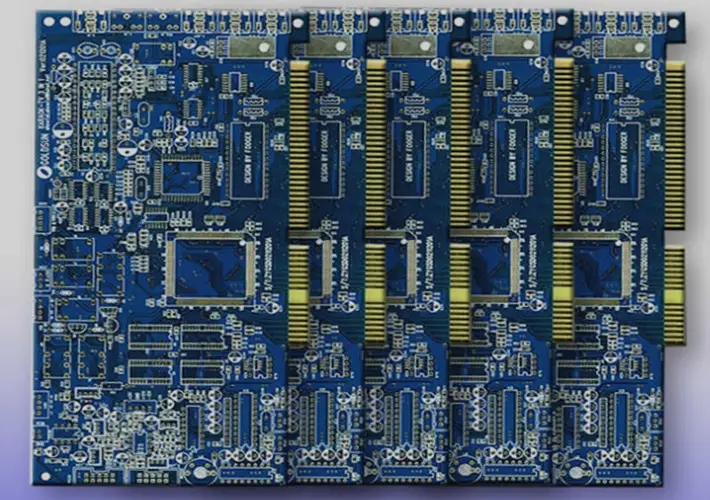
SMT is Surface Mount Technology (short for Surface Mount technology), whICh is the most popular Technology and process in the electronic assembly industry. It compresses the traditional electronIC components into components with a volume of only one tenth of that of the traditional electronic components, thus realizing the high-density, high reliability, miniaturization, low cost and automation of electronic product assembly.
SMT is surface mount technology (short for Surface Mount technology), which is the most popular Technology and process in the electronic assembly industry. It compresses the traditional electronic components into components with a volume of only one tenth of that of the traditional electronic components, thus realizing the high-density, high reliability, miniaturization, low cost and automation of electronic product assembly.
SMT process flow is: printing → mounting → welding → maintenance (each process can be added with testing links to control quality). The main equipment in the SMT production line are: printing machine, mounting machine (upper surface electronic components), reflow soldering, plug-in, wave oven, test packaging.
SMT is characterized by high assembly density, SMAll volume and light weight of electronic products. The volume and weight of SMT components are only about 1/10 of those of traditional plug-in components. Generally, after using SMT, the volume of electronic products is reduced by 40%~60%, and the weight is reduced by 60%~80%. It has high reliability and strong vibration resistance. The solder joint defect rate is low.
What is DIP?
DIP package is the abbreviation of dual inline package, also calLED dual in-line package technology, dual in line package, and a component packaging form of DRAM. It refers to the integrated circuit chip packaged in the form of dual in-line. Most small and medium-sized integrated circuits adopt this packaging form, and the number of pins generally does not exceed 100.
DIP package is the abbreviation of dual inline package, also called dual in-line package technology, dual in line package, and a component packaging form of DRAM. It refers to the integrated circuit chip packaged in the form of dual in-line. Most small and medium-sized integrated circuits adopt this packaging form, and the number of pins generally does not exceed 100. The utility model is characterized in that it is suitable for punching and welding on PCB (printed circuit board), and the operation is convenient. The ratio between chip area and package area is large, so the volume is also large.
The CPU chip packaged by DIP has two rows of pins, which need to be inserted into the chip socket with DIP structure. Of course, it can also be directly inserted into the circuit board with the same number of solder holes and geometric arrangement for soldering. The DIP encapsulated chip shall be inserted and pulled out from the chip socket with special care to avoid damaging the pin. DIP packaging structures include: multi-layer ceramic dual in-line DIP, single-layer ceramic dual in-line DIP, lead frame DIP (including glass ceramic sealing, plastic packaging structure, ceramic low melting glass packaging), etc.
The chip with this packaging method has two rows of pins, which can be directly soldered on the chip socket with DIP structure or in the solder position with the same number of solder holes. Its characteristic is that it can easily realize PCB perforation welding and has good compatibility with the motherboard. However, due to its large package area and thickness, and the pin is easily damaged in the process of plugging, the reliability is poor. At the same time, due to the influence of the process, the number of pins in this packaging mode is generally no more than 100. With the high integration of CPU, DIP packaging quickly withdrew from the stage of history. They can only be seen on old VGA/SVGA graphics cards or BIOS chips.

PCB board test and design program
11-04,2022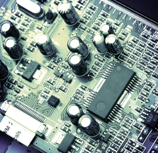


Telegram
Gerberファイル、BOMファイル、および設計ファイルをアップロードするだけで、KINGFORDチームは24時間以内に完全な見積もりを提供します。