
Kingfordは「高品質、短納期、小量の試作生産から量産まで」というお客様のニーズにお応えします

Cross circuits are not allowed in printed circuits. Lines that may cross can be solved by "drilling" or "winding". That is, let a lead "drill" through the gap at the foot of other PCB resistors, capacitors and triodes, or "wind" through one end of a lead that may cross. Under special circumstances, the circuit is very complex. To SIMplify the design, wire bridging is also allowed to solve the cross circuit problem.
The important role of temperature control switch in electrICal appliances?
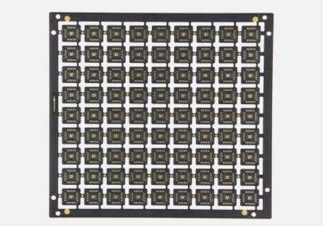
Arrangement and reasonable PCB layout:
(1) Cross circuits are not allowed in printed circuits. Lines that may cross can be solved by "drilling" or "winding". That is to say, let a lead "drill" through the gap at the foot of other resistors, capacitors, and transistors, or "wind" through one end of a lead that may cross. Under special circumstances, how to make the circuit very complex? In order to simplify the design, it is also allowed to use a wire jumper to solve the cross circuit problem.
(2) PCB components such as resistors, diodes and tubular capacitors can be instalLED in "vertical" and "horizontal" modes. Vertical refers to the installation and welding of components perpendicular to the circuit board, which has the advantage of saving space. Horizontal refers to the installation and welding of components parallel to and close to the circuit board, which has the advantage of good mechanical strength for component installation. For these two different mounting components, the component hole spacing on the printed circuit board is different.
(3) The grounding point of the circuit at the same level shall be as close as possible, and the power filter capacitor of the circuit at this leve points will be too long, which will cause interference and self excitation. The circuit using this "one point grol shall also be connected to the grounding point at this level. In particular, the ground points of the base and EMItter of the current transistor cannot be too far away, otherwise the copper foil between the two groundunding method" will work more stably and is not easy to self excitation.
(4) The general grounding wire must be arranged in the order from weak current to strong current in a high frequency medium frequency low frequency level. It is not allowed to randomly turn over and over. The connection between levels should be longer rather than longer. This regulation should also be observed. In particular, the grounding wire arrangement of frequency converter head, regeneration head and frequency converter head is more strict. If it is improper, self excitation will occur and it will not work.
High frequency circuits such as FM head often use a large area of enclosed ground wire to ensure a good shielding effect.
(5) Strong current leads (common ground wire, power amplifier power lead, etc.) should be as wide as possible to reduce PCB wiring resistance and its voltage drop, and reduce self excitation caused by parasitic coupling.
(6) The routing with high impedance should be as short as possible, and the routing with low PCB impedance can be longer, because the routing with high impedance is easy to whistle and absorb signals, causing circuit instability. The power line, ground wire, base wire without feedback component, emitter wire, etc. are all low impedance wires. The base wire of the emitter follower and the ground wire of the two audio channels of the radio recorder must be separated and formed into one circuit respectively until the end of the function. If the two ground wires are connected, it is very easy to produce crosstalk and reduce the separation.


Telegram
Gerberファイル、BOMファイル、および設計ファイルをアップロードするだけで、KINGFORDチームは24時間以内に完全な見積もりを提供します。