
Kingfordは「高品質、短納期、小量の試作生産から量産まで」というお客様のニーズにお応えします

プリント基板設計の人材レベルと一次基板設計技術能力
能力要件:
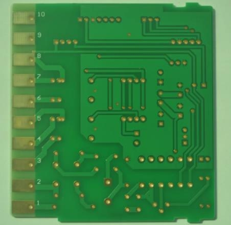
DIP10等の簡易パッケージも製作可能です。
少なくとも 1 つの PCB 設計ソフトウェアの基本的な操作をマスターし、配線の線幅や間隔などの簡単なルールを作成できる。
部品点数100点、ネットワーク数200点以下のPCBをより合理的かつ整然と配置・配線できます。
100% のルーティングと DRC パスを完全に達成するために、手動または自動で配線し、他の人または自分で定義したルールの下で変更することができます。
機械構造と熱設計の基礎知識。
両面基板配線の基本要件をマスターします。
仕事内容:
シンプルな PCB の設計と変更 (シンプルな構造のフロント パネル、シングル チップ マイクロコンピュータの小型システム ボードなど)。
複雑な PCB 内の特定の部品の配線。
自己設計 PCB に関連するデバッグ;
関連する開発およびデバッグ ログを書き込みます。
運用義務:
PCBの設計部分を担当。
ジュニア PCB エンジニア
能力要件:
マニュアルと物理オブジェクトに従って、ライト付きの RJ-45 シートなどの複雑なパッケージを作成し、形状、パッド、およびその他の寸法が完全に正しいことを確認できます (少なくとも、物理オブジェクトに従って挿入できます)。
少なくとも 1 つの PCB 設計ソフトウェアに精通しており、詳細な配線規則を独立して、または指導の下で作成できる。
400 個のコンポーネントと 1000 個以下のネットワークを備えた単層、2 層、および多層 PCB の合理的かつ整然としたレイアウトと配線を実行でき、熱設計、構造設計、電磁適合性設計、美学およびその他の側面の要件を考慮することができます。 レイアウトおよび配線プロセスのいつでも。 確信が持てない場合は、時間内に上位レベルの PCB エンジニアに相談するか、話し合うことができます。
Be able to skillfully route and modify manually or automatICally under other people's or self determined rules, and achieve 100% routing and DRC pass completely. There are basically no problems such as line width bottleneck, inner layer islands, etc. During the routing process, a SMAll number of low-level errors in principle design can be seen and raised, and the pins and doors can be exchanged correctly, and the network table and schematic diagram can be modified correctly;
Can correctly import and export mechanical drawings and basically understand the structural dimension requirements;
Be able to carry out some high-speed and analog PCB design under the rules or guidance of others and basically stable;
The silk screen MARK is clear and clear, and can independently complete GERBER and other design output work and proofread;
Have basic knowLEDge of manufacturability and apply it to practice. More than 50% of the designed boards can be used for production.
job content:
Design and modification of more complex PCB (such as boards other than CPU boards in the scheduling machine, 16 screen splitter boards, etc.);
Wiring of specified parts in complex PCB;
Debugging related to self-designed PCB;
Work guidance for all lower level PCB engineers;
Write relevant development and debugging logs;
When necessary (it means that you do not have corresponding design tasks for a certain period of time, or the design work time of a PCB is urgent, and you must transfer or strengthen the designers, the same below), take any low-level PCB engineer's job. PCB factory: explain the PCB design ability that entry-level PCB engineers and junior PCB engineers need to master.
operating duty:
Responsible for the design part of PCB. PCB assembly, PCB design, and PCB processing manufacturers introduce people's level of pcb design and primary pcb design engineering capabilities.
PCB設計の中級PCB技術者 PCB設計工学の能力
12-01,2022


Telegram
Gerberファイル、BOMファイル、および設計ファイルをアップロードするだけで、KINGFORDチームは24時間以内に完全な見積もりを提供します。