
Kingfordは「高品質、短納期、小量の試作生産から量産まで」というお客様のニーズにお応えします

Widely used in circuit board design
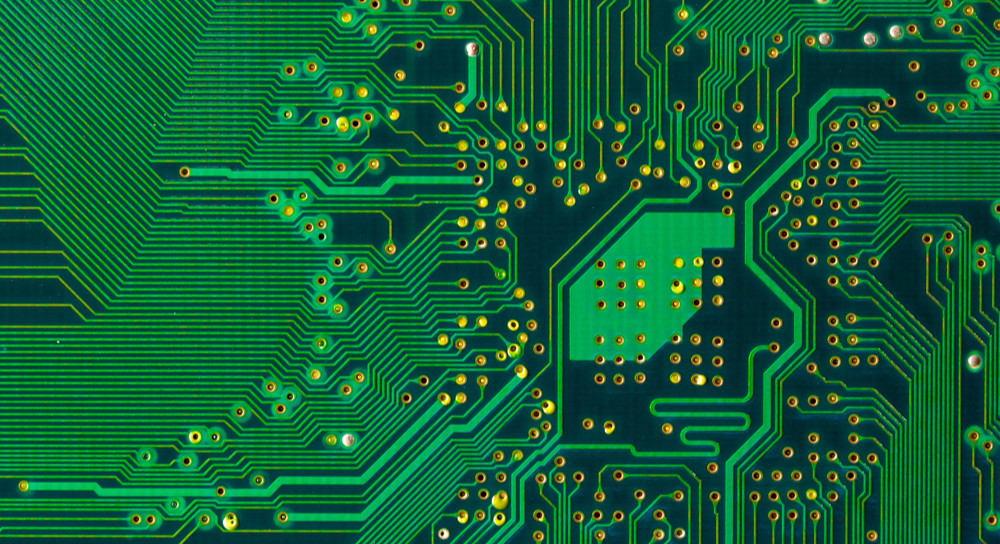
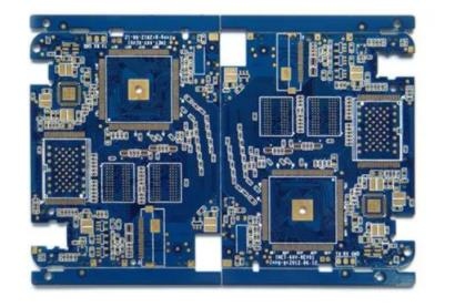
Generally, conductive patterns made of printed circuit boards, printed PCB components or the combination of the two on insulating materials are calLED printed circuits according to the predetermined design of PCB A conductive pattern that provides electrICal connection between components on an insulating substrate is called a printed circuit board circuit In this way, the printed circuit or the finished board of the printed circuit is called the printed circuit board, also called the printed circuit board or the printed circuit board PCBs can not be separated from almost all electronic equipment that our circuit board design company can see, from electronic watches, abacuses, general-purpose computers, computers, communication electronic equipment, military weapon systems, as long as there are integrated circuits and other electronic equipment For equipment, PCBs are used for power interconnection between them It provides mechanical support for the fixed assembly of various electronIC components (such as integrated circuits), realizes the wiring and electrical connection or electrical insulation between various electronic components (such as integrated circuits), and provides the required electrical characteristics, such as characteristic impedance At the same time, it provides a welding mask pattern for automatic welding; Provides character recognition and graphics, inspection, and maintenance for component insertion How are PCBs made? We can see a flexible film (a flexible insulating substitute) printed with a silver white (silver paste) conductive pattern and a healthy bit pattern Because the general screen printing method can obtain this pattern, we call this printed circuit board flexible silver paste printed circuit board The printed circuit boards, graphics cards, network cards, and data machines on various computer mainboards. The sound cards we see in the computer city are different from household appliances The substitute used in it is made of paper base (usually used for single sided) or glass cloth base (usually used for double sided and multilayer), pre impregnated with phenolic or epoxy resin, the surface layer is laminated with copper film on one side or both sides, and then laminated and cured This kind of circuit board copper clad material is called rigid board Then make a printed circuit board, which we call rigid printed circuit board We call single-sided printed circuit boards single-sided printed circuit boards and printed circuit boards with printed circuit patterns on both sides The printed circuit board formed by metallization of the double side interconnecting holes is called the double side board If one double-sided PCB is used as the inner layer, two single-sided PCB is used as the outer layer, or two double-sided PCB is used as the inner layer, and two single-sided PCB is used as the outer layer, the positioning system and insulation bonding materials are alternated together, and the PCB with conductive patterns interconnected according to design requirements is divided into four or six layer PCB, also known as multilayer PCB There are now 100 layers of practical printed circuit boards
The production process of polychlorinated biphenyls is more complex, which involves a wide range of processes, from SIMple mechanical processing to complex mechanical processing, common chEMIcal reactions, photochemistry, electrochemistry, thermochemistry and other processes, CAD CAM and other knowledge. In addition, there are many process problems in the production process, and new problems will be encountered from time to time Some problems disappear without finding the cause Because the production process is a discontinuous assembly line, any problem in any link will lead to the shutdown of the entire production line Or because of the large amount of waste materials, if printed circuit boards are scrapped, they cannot be recycled The working pressure of process engineers is relatively high. In retrOSPect, many engineers have left the industry and turned to PCB equipment or material suppliers for sales and technical services
Circuit board

In order to further understand PCBs, we need to understand the production process of common single-sided and double-sided printed circuit boards and ordinary multilayer boards to deepen our understanding of them. Single sided rigid printed circuit board: - single sided copper clad plate - blanking - (brushing, drying) - drilling or punching - screen printed circuit anti etching pattern or using dry film - curing inspection and repair plate - etching copper - removing corrosive printing, drying - brushing, drying - screen printed solder mask graphics (often using green oil), UV curing - screen printed character MARKing graphics, UV curing - preheating, punching and molding - power on, short circuit test - brushing Drying - precoating welding antioxidants (drying) or spraying tin and hot air leveling - inspection and packaging - finished products leaving the factory.
Double sided rigid PCB printed boards: - double-sided copper clad boards - blanking - stacking - CNC drilling - inspection, deburring and brushing - chemical plating (through hole metallization) - (full plate electroplating of thin copper) - inspection and scrubbing - screen printing of negative circuit patterns, curing (dry film or wet film, exposure, development) - inspection, Repair - circuit pattern electroplating - tin plating (anti-corrosion nickel/gold) - removing printed materials (photosensitive film) - etching copper - (removing tin) - cleaning and scrubbing screen printing solder mask patterns commonly used thermal curing green oil (photosensitive dry film or wet film, exposure, development, thermal curing, commonly used photosensitive thermosetting green oil) - cleaning, drying screen printing and marking text and graphics, curing - (tin spraying or organic solder resistance) - shape treatment cleaning Dry power continuity inspection and packaging of finished products.
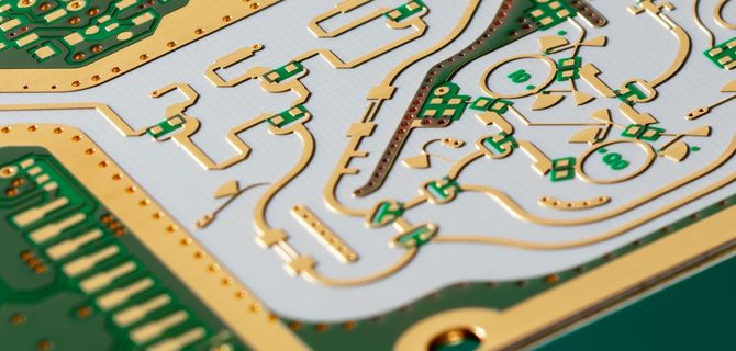
Process flow of through hole metallization method for manufacturing multilayer plates - double-sided cutting of inner copper clad plate - brushing - drilling positioning holes - pasting photoresist dry film or coating photoresist - exposure - development - etching and removal of film - inner layer roughening, Deoxygenation - inner layer inspection - (outer single-sided CCL circuit production, B-level bonding sheet, plate bonding sheet inspection, drilling positioning hole) - lamination - CNC drilling - hole inspection - hole pretreatment and chemical copper plating - thin copper plating on the whole board - electroplating inspection - pasting photoresist electroplating dry film or coating photoresist plating agent - surface layer - bottom plate exposure - development, Repair circuit board - circuit pattern electroplating - tin lead alloy electroplating or nickel/gold electroplating - film removal and etching - inspection - screen printed solder mask or photo solder mask graphics - printed character graphics - (hot air leveling or organic solder mask) - CNC cleaning shape - cleaning, drying - power switch detection - finished product inspection - packaging and delivery. It can be seen from the process flow chart that the Multilayer board process is developed on the basis of the double-sided metallization process. In addition to double-sided process, it has several unique contents: metallized hole inner layer interconnection, drilling and epoxy drilling, positioning system, lamination and special information.
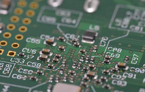
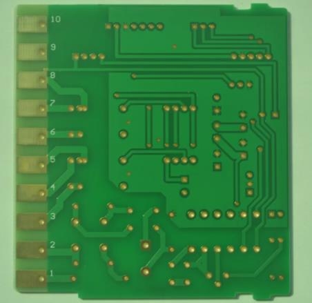
Our common computer board is basically a double-sided printed pcb circuit board based on epoxy resin glass cloth One side is used for inserting components and the other side is used for soldering component pins It can be seen that the solder joints are very regular These solder joints - discrete solder surfaces of component pins - are called pads Why are other copper wire patterns not tinned? Because except for pads and other parts, the surfaces of other parts have wave soldering mask Most of the solder mask on the surface is green, and a few are yellow, black, blue, etc, In PCB industry, solder resist is usually called green oil Its function is to prevent bridge during wave soldering, improve welding quality and save solder It is also a permanent protective layer for printed boards, which can prevent moisture, corrosion, mold and mechanical scratches From the outside, the smooth and bright green solder mask is a kind of green oil, which has photosensitivity and thermal curing property to the film on the circuit board Not only does the appearance look better, but also the PCB pad is more accurate, which improves the reliability of PCB solder joints


Telegram
Gerberファイル、BOMファイル、および設計ファイルをアップロードするだけで、KINGFORDチームは24時間以内に完全な見積もりを提供します。