
Kingfordは「高品質、短納期、小量の試作生産から量産まで」というお客様のニーズにお応えします

How to improve PCB EMI through component placement?
After designing the circuit structure and devICe position, PCB EMI control is very important to the overall design How to avoid interference in PCB electromagnetic switching power supply has become a topic of great concern for developers
The component layout practice has proved that even if the PCB schematic design is correct, the Printed Circuit Board Design is incorrect, which will adversely affect the reliability of electronic equipment For example, if two thin parallel lines of the printed circuit board are close together, the signal waveform will be delayed and reflective noise will be formed at the end of the transmission line The efficiency is reduced, so you should pay attention to the correct method when designing the printed circuit board
Each switching power supply has four current circuits:
(1) AC circuit of power switch;
(2) AC circuit of output rectifier;
(3) Current loop of input signal source;
(4) Output load current loop.
The input circuit charges the input capacitor through approximate DC current, and the filter capacitor is mainly used for broadband energy storage; SIMilarly, the output filter capacitor is also used to store high-frequency energy from the output rectifier and eliminate the DC energy of the output load circuit. The terminals of input and output filter capacitors are very important. The input and output current circuits can only be connected to the power supply from the terminals of the filter capacitor; If the connection between the input/output circuit and the power switch/rectifier circuit cannot be connected to the capacitor, connect the terminal directly, and the AC energy will be radiated to the environment through the input or output filter capacitor.
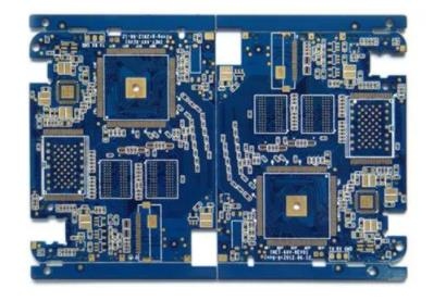
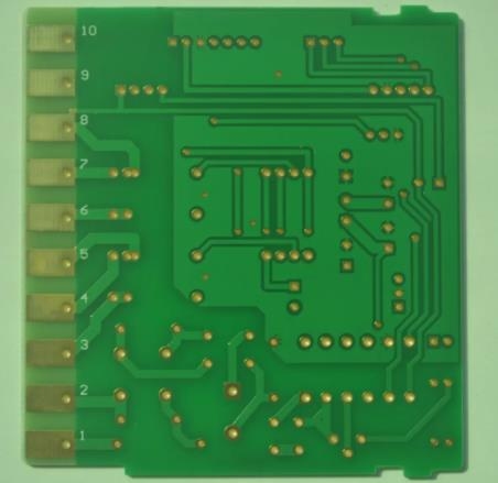
Circuit board

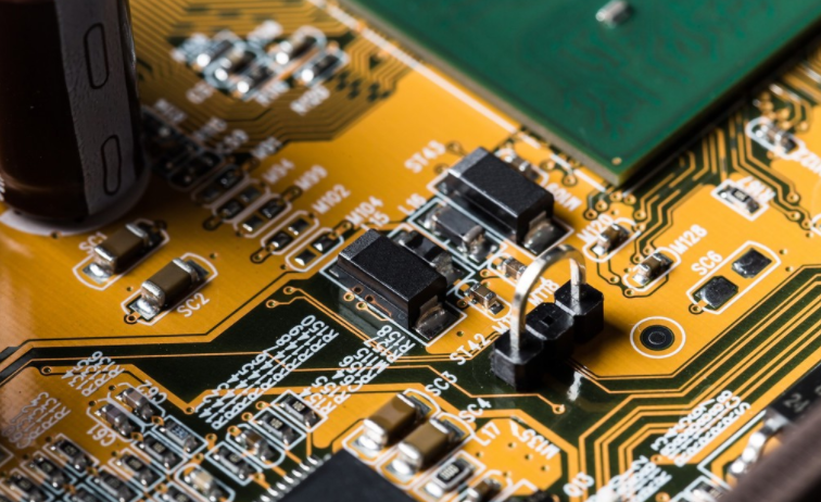
The AC circuit of the power switch and the AC circuit of the rectifier contain high amplitude ladder current. The harmonIC components of these currents are very high. The frequency is much greater than the fundamental frequency of the switch. The peak amplitude can be up to 5 times the amplitude of continuous input/output DC current. The transition time is usually about 50ns. These two circuits are most vulnerable to electromagnetic interference. These AC circuits must be arranged before other printed lines in the power supply. The three main components of each circuit are filter capacitor, power switch or rectifier, inductor or transformer. Place them next to each other and adjust the position of the components so that the current path between them is as short as possible. The best way to establish a switching power supply layout is similar to its electrical design. The optimal design process is as follows:
Place the transformer
Design power switch current circuit
Design current circuit of output rectifier
Control circuit connected to AC power circuit
When designing the input current source circuit and input filter and designing the output load circuit and output filter according to the functional unit of the circuit, the following principles must be met when arranging all components of the circuit:
(1) First, consider the PCB size When the PCB size is too large, the printed lines will be very long, the impedance will be increased, the noise resistance will be reduced, and the cost will be increased; If the PCB size is too SMAll, the heat dissipation is poor, and adjacent circuits are vulnerable to interference The best shape of the circuit board is rectangle, with the aspect ratio of 3:2 or 4:3. The distance between the components at the edge of the circuit board and the edge of the circuit board is usually not less than 2mm
(2) When placing the equipment, consider the subsequent welding, not too intensive.
(3) Centering on the core components of each functional circuit, the layout is carried out around them. The components shall be uniformly, orderly and compactly arranged on the PCB to minimize and shorten the leads and connections between components. The decoupling capacitor shall be as close to the VCC of the components as possible.
(4) For high frequency circuits, the distribution parameters between components must be considered. In general, circuits should be arranged in parallel as far as possible. In this way, it is not only beautiful, but also easy to install, weld and mass produce.
(5) Arrange the position of each functional circuit unit according to the circuit flow, so that the layout is convenient for signal flow, and the signals are kept in the same direction as far as possible.
(6) The first principle of layout is to ensure the wiring speed. When moving equipment, pay attention to the connection of flying wires, and put the equipment with connection relationship together.
(7) Reduce the loop area as much as possible to suppress the radiated interference of switching power supply


Telegram
Gerberファイル、BOMファイル、および設計ファイルをアップロードするだけで、KINGFORDチームは24時間以内に完全な見積もりを提供します。