
Kingfordは「高品質、短納期、小量の試作生産から量産まで」というお客様のニーズにお応えします

PCB power and non electrICal safety clearance
1 Spacing between wires
In terms of mainstream processing capacity, PCB manufacturers are concerned that the minimum spacing between conductors should not be less than 4mil The minimum line distance is also the line to line and line to pad distances From the production point of view, if possible, the larger the better. The more common is 10mil
2. Pad hole diameter and pad width
As far as the processing capacity of mainstream PCB manufacturers is concerned, if the pad aperture is mechanically drilLED, the minimum value should not be less than 0.2 mm, and if laser drilling is used, the minimum value should not be less than 4 mil. Aperture tolerance varies from plate to plate and can be controlled within 0.05mm generally. The minimum pad width should not be less than 0.2mm.
3. Distance between base plate and base plate
As far as the processing capacity of mainstream PCB manufacturers is concerned, the distance between pads should not be less than 0.2mm.
4. Distance between copper sheet and plate edge
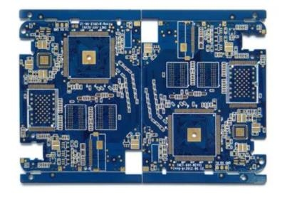
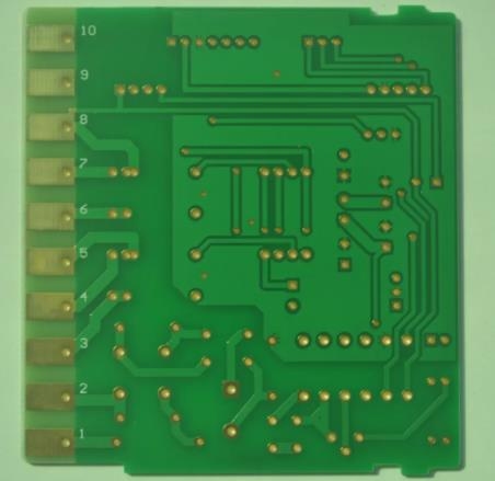
Circuit board

The distance between the charged copper sheet and the edge of PCB board should be no less than 0.3mm. Set spacing rules on the design Rule board Outline page.
If it is a large area copper, it usually needs to be retracted from the edge of the circuit board, usually set as 20mil In the PCB design and manufacturing industry, under normal circumstances, due to the mechanical factors of the finished circuit board, or to avoid curling or power short circuit due to the exposed copper sheet on the board edge, engineers often spread copper blocks on a large area, shrinking 20 mils relative to the circuit board edge, instead of laying copper sheets on the edge of the circuit board
There are many ways to deal with this copper shrinkage, such as drawing a forbidden layer at the edge of the board, and then setting the distance between copper laying and the forbidden. Here is a SIMple way to set different safety distances for copper paving objects. For example, the safety distance of the whole board is set as 10mil, and the copper laying is set as 20mil, which can achieve the effect that the board edge shrinks inwards by 20mil. Remove the dead copper that may appear in the equipment.
Non electric power related safety clearance
1. Character width, height, and spacing
The text film cannot be changed during processing, but the character line width of D code SMAller than 0.22mm (8.66mil) is thickened to 0.22mm, that is, the character line width L=0.22mm (8.66mil), the width of the whole character W=1.0mm, the height of the whole character H=1.2mm, and the spacing between characters D=0.2mm. When the text is smaller than the above standard, processing and printing will become blurred.
2. Clearance between vias
The distance between vias (VIA) and vias (hole edge to hole edge) should preferably be greater than 8mil.
3. Distance from silk screen to mat
It is not allowed to cover the mat with wire mesh. Because if the screen is covered by the mat, the screen will not be tinned during the tinning process, which will affect the installation of components. Generally speaking, the plate factory needs to reserve 8mil of space. If PCB area is really limited, 4mil spacing is almost unacceptable. If the silk screen accidentally covers the bonding pad during the design process, the Circuit board factory will automatically remove the silk screen left on the bonding pad during the manufacturing process to ensure that the bonding pad is tinned.
Of course, the specific conditions were analyzed in detail during the design process. Sometimes the wire mesh is intentionally close to the pad, because when two pads are very close, the middle wire mesh can effectively prevent short circuit of solder joints during welding. This is another matter.
4. Mechanical 3D height and level spacing
When installing equipment on PCB, consider whether it will conflict with other mechanical structures in horizontal direction and space height Therefore, during the design, the adaptability between components, the PCB product and the product shell, as well as the space structure must be fully considered, and a safe distance must be reserved for each target object to ensure that there is no conflict in the space
The above is the explanation given by the editor of pcb circuit board company.
If you want to know more about PCBA, you can go to our company's home page to learn about it.
In addition, our company also sells various circuit boards,
High Frequency Circuit Board and SMT chip are waiting for your presence again.


Telegram
Gerberファイル、BOMファイル、および設計ファイルをアップロードするだけで、KINGFORDチームは24時間以内に完全な見積もりを提供します。