
Kingfordは「高品質、短納期、小量の試作生産から量産まで」というお客様のニーズにお応えします


How to deal with PCB process negative deformation
It is used for PCB copy board. A little carelessness may cause deformation of the backplane If there is no improvement, it will affect the quality and effICiency of the PCB copy board If it is discarded directly, it will cause costs In relation to loss Here are
some ways to correct the deformation of the bottom plate.
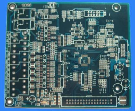
PCB board

1. Splicing method
For graphics with SIMple lines, large line width and spacing, and irregular deformation, cut off the deformed part of the negative film, re drill according to the hole position of the drilling test plate, and then copy them Of course, this is for
deformed lines. Easy to understand, large line width and spacing, and irregular deformation figures; It is not applicable to negative films with high linear density, line width and spacing less than 0. 2mm You need to pay as little as possible to
damage the wires and not the pads. When modifying the version after splicing and copying, pay attention to the correctness of the connection relationship This method is suitable for the film that is not too densely packed and the film deformation
of each layer is inconsistent. This effect is especially obvious for the correction of the solder mask of Multilayer board and the mask of power supply layer
2. Copy board to change the hole position method
Under the condition of mastering the operating technology of the digital programming instrument, first compare the negative film and the drilling test plate, measure and record the length and width of the drilling test plate, and
then use the digital programming instrument according to its length and width. The size of the deformation, adjust the hole position, and adjust the adjusted drilling test plate to adapt to the deformed negative film The advantage of this method is
That it defines the cumbersome work of editing negatives, and can ensure the integrity and quality of graphics The disadvantage is that the correction of the negative film with very serious local deformation and uneven deformation is not
effective. To use this method, you must first master the operation of digital programming instruments The out of tolerance hole position should be reset to
ensure the performance. This method is suitable for correcting films with dense lines or uniformly deformed films of each layer
3. Pad overlap method
Enlarge the holes on the test board into pads to overlap and deform the circuit piece to ensure the technical requirements of the ring width. After overlapping replication, the cushion is elliptical, and after overlapping replication, the straight line and disk edge are halo and deformed
If users have very strict requirements on the appearance of PCB, please use it carefully This method is applicable to films with line width and spacing greater than 0 30mm, and the pattern lines are not too dense
4. Photography
Just use the CAMera to enlarge or reduce the deformed graphics. Normally, the film loss is relatively high, and it requires multiple debugging to obtain a satisfactory circuit diagram The focus should be accurate when taking pictures to
prevent the lines from being deformed. This method is only applicable to silver salt film. It can be used when the test panel is not convenient for drilling again and the deformation rate of the film in the length and width directions is the same
5. Hanging method
In view of the physical phenomenon that the negative film changes with the environmental temperature and humanity
negative film has been deformed before copying. After copying, the possibility of deformation is very SMAll Other measures required for deformed film Because the negative film will change with the change of
Environmental temperature and humidity, when hanging negative films, ensure that the humidity and temperature of the hanging place are consistent with that of the workplace, and it needs to be in a ventilated and dark environment to
prevent the negative film from being contaminated. This method is applicable to undeformed negative film and can also prevent the negative film from deforming after copying
The above is the explanation given by the editor of pcb circuit board company.
If you want to know more about PCBA, you can go to our company's home page to learn about it.
In addition, our company also sells various circuit boards,
High Frequency Circuit Board and SMT chip are waiting for your presence again.


Telegram
Gerberファイル、BOMファイル、および設計ファイルをアップロードするだけで、KINGFORDチームは24時間以内に完全な見積もりを提供します。