
Kingfordは「高品質、短納期、小量の試作生産から量産まで」というお客様のニーズにお応えします

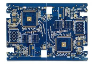
Some necessary knowLEDge of BGA components in PCB design!
SMT technology conforms to the development trend of miniaturization and lightness of intelligent electronIC products, laying a foundation for realizing the lightness, thinness, short and SMAll of electronic products. SMT technology also beCAMe mature in the 1990s. However, with the rapid development of electronic products towards portable/miniaturization and networking, higher requirements are put forward for electronic assembly technology, among which BGA (Ball Grid Array Package) is a high-density assembly technology that has entered the practical stage.
The research of BGA technology started in the 1960s and was first adopted by IBM in the United States. But it was not until the early 1990s that BGA really entered the practical stage. Due to the previously popular high-density pin devices SIMilar to QFP package, the limitation of its fine spacing is that thin leads are easy to bend, brittle and break, and the requirements for coplanarity and mounting accuracy between leads are very high. BGA technology adopts a new design thinking mode. It adopts a structure that hides round or cylindrical points under the package, with large lead spacing and short lead length. In this way, BGA eliminates the defects of coplanarity and warpage caused by lead wire problems in fine pitch devices.
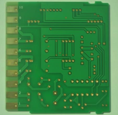
BGA is a commonly used component on PCB, usually 80% of high-frequency signals and special signals will be pulled out from this type of packaging Footprint. Therefore, how to handle the routing of BGA devices will have a great impact on important signals.
How to route BGA devices?
When wiring ordinary BGA devices, the general steps are as follows:
1. First, determine the number of boards required according to the number of bonding pads of BGA devices, and then conduct the lamination design.
2. Then fan out the main device BGA (that is, lead a small segment of line from the bonding pad, and then place a via at the end of the line to reach another layer).
3. Then escape wiring from the via to the edge of the device, and fan out through the available layers until all pads are escape wiring completed.
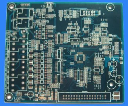
The cabling during fanout and escape is carried out according to the applicable design rules. It includes fanout control Fanout Control rule, wiring width RouTIng Width rule, wiring via method RouTIng Via Style rule, wiring layer RouTIng Layers rule and Electrical Clearance rule. If the rules are set unreasonably, for example, the number of layers is not enough, the unlimited width is too wide to walk out, the through-hole is too large to drill, the spacing violates the safety distance, etc., the fan out will fail. When the fanout operation does not respond, please check your rule settings and make appropriate modifications. Fanout can succeed only after there are no problems. As shown in the figure below. The routing color of each layer is different.
The Fan Out dialog box allows you to control and define the options related to fan out and escape routing, and some options are used for blind holes (holes between layer pairs can be set in the Layer Stack Manager dialog box of the stack manager). Other options include whether the other two rows and columns are fanned out at the same time as the internal rows and columns, and whether only the pads assigned to the network are fanned out.
How to wire extremely small BGA (0.4mm spacing) devices?
Because of the complexity of BGA's processing technology, in addition to its functional design, the most important thing in the design phase is to communicate with PCB manufacturers and chip assembly plants. Different manufacturers have different processes and capabilities. For processing and manufacturing costs, proofing and batch production are also different. Therefore, more importantly, BGA design should also consider the processing cost, the yield rate of production and other factors.
Today's BGA is not a fuel saving lamp. This kind of BGA module design has refreshed the bottom line and belongs to the category of minimum processing capacity. Let's take a look at its parameter characteristics:
BGA pad 0.3mm (12mil)
BGA center to center spacing is 0.4mm (16mil)
The X and Y directions of pad and pad edge to edge are 0.1mm (4mil).
The diagonal direction of pad and pad edge is 0.27mm (10.8mil)
Wiring solution for extremely small BGA (0.4mm spacing) devices Conclusion:
Technically, it can only be used for multi-layer board wiring with more than 4 layers. BGA devices have 0.4mm ball pitch, 0.3mm ball pad diameter, and need laser blind holes for interconnection (the minimum laser processing aperture capacity is 0.1mm). According to the design requirements, it is possible to do second-order interconnection; And the design of the hole in the disc is required.
PCB manufacturers, PCB designers and PCBA manufacturers will explain some necessary knowledge about BGA components in PCB design.


Telegram
Gerberファイル、BOMファイル、および設計ファイルをアップロードするだけで、KINGFORDチームは24時間以内に完全な見積もりを提供します。