
Kingfordは「高品質、短納期、小量の試作生産から量産まで」というお客様のニーズにお応えします

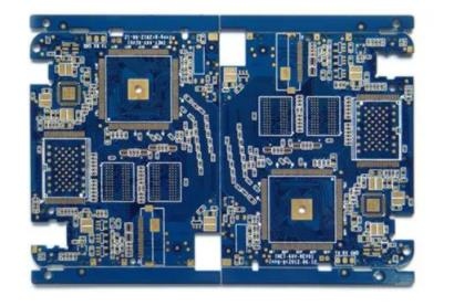
DetaiLED explanation of several major mistakes to be vigilant in circuit board design
We often find that there are mistakes in some rules or principles we take for granted. ElectronIC engineers also have such examples in circuit design. Xiao Bian summarized the common mistakes in circuit design and hoped that everyone could avoid them when designing.
Myth 1: This PCB has low design requirements, so we can use thinner lines or hand them over to the software for automatic wiring
Comments: Automatic wiring will inevitably occupy a larger PCB area and generate many times more vias than manual wiring. Among products in large batches, the factors considered by PCB manufacturers for price reduction, apart from business factors, are the line width and the number of vias. They respectively affect the yield of PCB and the consumption of drill bits, saving the cost of suppliers, and thus finding reasons for price reduction.
Myth 2: How to deal with these unused I/O ports of CPU and FPGA - vacant or ignored
Comment: If the unused I/O port is suspended, a little interference from the outside may become an input signal that oscillates repeatedly. The power consumption of MOS devices basically depends on the number of flips of the gate circuit. If you pull it up, each pin will also have microamp current, so the best way is to set it as an output (of course, no other driving signals can be connected outside)
Error 3: These bus signals need to be pulled with a resistor
Comment: There are many reasons why signals need to be pulled up and down, but not all of them need to be pulled up and down. Pull up and down the resistance to pull a SIMple input signal, and the current will be less than tens of microamps. But pull a driven signal, and the current will reach milliampere level. Today's systems often use 32 bits of address data, and possibly 244/245 isolated buses and other signals. If you pull up, several watts of power consumption will be consumed by these resistors.
Mistake 4: Randomly handle redundant gates of FPGA
Comment: The power consumption of FGPA is proportional to the number of flip-flop used and the number of flips, so the power consumption of the same type of FPGA in different circuits at different times may vary by 100 times. Minimizing the number of flip flops is the fundamental way to reduce FPGA power consumption.
Myth 5: The power consumption of these SMAll chips is very low, so it is unnecessary to consider
Comments: It is difficult to determine the power consumption of a chip that is not too complex internally. It is mainly determined by the current on the pin. An ABT16244 consumes less than 1 mA without a load, but its indicator is that each pin can drive a load of 60 mA (such as matching a resistance of tens of ohms). That is, the maximum power consumption of a full load can reach 60 * 16=960mA. Of course, the power supply current is so large that the heat falls on the load.
Myth 6: There are so many control signals in the memory. I only need to use OE and WE signals on this board. Just ground the chip selection, so that the data will come out much faster during the read operation
Comment: The power consumption of most memories will be more than 100 times greater when the chip selection is valid (regardless of OE and WE) than when the chip selection is invalid. Therefore, CS should be used to control the chip as much as possible, and the width of the chip selection pulse should be shortened as much as possible when other requirements are met.
Myth 7: Why are these signals overshoot? As long as the match is good, it can be eliminated
Comments: Except for a few specific signals (such as 100BASE-T and CML), there are overshoots. As long as they are not very large, they do not need to be matched, even if the matching is not the best. For example, the output impedance of TTL is less than 50 ohms, and some even 20 ohms. If such a large matching resistance is also used, the current will be very large, the power consumption will be unacceptable, and the signal amplitude will be too small to use. In addition, the output impedance of general signals at high output level and low output level is not the same, and there is no way to achieve complete matching. Therefore, the matching of TTL, LVDS, 422 and other signals is acceptable as long as overshoot is achieved.
Myth 8: Reducing power consumption is a matter for hardware personnel, not software
Comment: The hardware is just a stage, but the software is the singer. The access to almost every chip on the bus and the overturning of every signal are almost controlled by the software. If the software can reduce the number of accesses to external memory (use more register variables, use more internal CACHE, etc.) Timely response to interrupts (interrupts are usually low level and have pull-up resistors) and other specific measures for specific boards will make a great contribution to reducing power consumption.
circuit board manufacturers, circuit board designers and PCBA manufacturers explain to you several major mistakes that need to be vigilant in circuit board design.


Telegram
Gerberファイル、BOMファイル、および設計ファイルをアップロードするだけで、KINGFORDチームは24時間以内に完全な見積もりを提供します。