
Kingfordは「高品質、短納期、小量の試作生産から量産まで」というお客様のニーズにお応えします

Other design rules and required data of circuit board assembly
The Circuit board manufacturer, circuit board designer and PCBA manufacturer explain other design rules and required data of Circuit board assembly
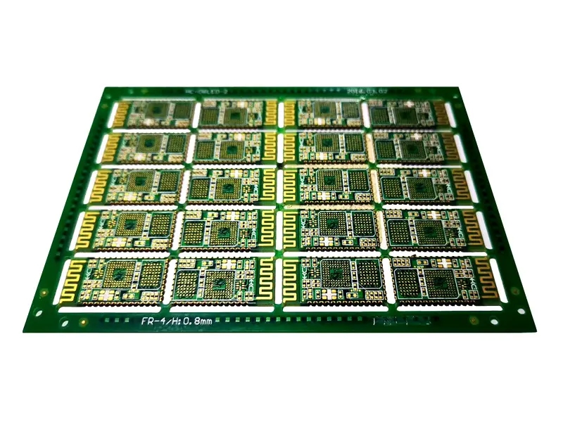
A 1.6mm or 2.4mm interval shall be reserved between each unit board in the panel to facilitate the division of Router or Punch. If a width less than 1.6mm is adopted, it is necessary to consider whether the equipment is suitable for such SMAll gaps.
2. On the four corners of the panel, design the tool holes that do not need plating. The entire panel shall ensure at least two holes, with the hole size of 3.05 ± 0.05mm. The center of the hole should be positioned at the corner of PCB, 5mm in X and Y directions respectively.
3. Fillets or chamfers with a radius of 5mm shall be designed on the four corners of the panel to prevent jamming on the rail transmission belt.
4. The panel design must ensure that the distance between the edge of the reference point (including the green oil opening) and the panel edge is at least 5mm. The reference points on both sides should not be placed symmetrICally, so that PCB can be prevented from entering the machine in reverse through the identification function of the device itself.
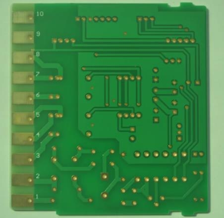
5. A direction sign can be designed at the edge of the panel, such as the sEMIcircular hole at the edge of the figure below, to prevent PCB from being in the wrong direction during production.
6. The maximum contour tolerance of PCB assembly shall be controlLED within 0.05mm.
7. Data required for completion of panel design
If you want to design a good panel drawing, you must have enough information to support it, otherwise it may cause subsequent SMT assembly or panel splitting quality problems due to unreasonable panel design. To complete a qualified panel design, the following data information is usually required.
Gerber file, including PCB component distribution, considering panel spacing and connection point placement position;
Outline drawing of PCB to understand the overall dimensions and specifications of PCB;
The specification of large components, especially plate edge components, requires the design of panel spacing, avoidance, etc.
4. Impact of poor panel design on production
In practical work, there are often some problems in panel design for various reasons, which may lead to production failure and difficulty in panel splitting.
The components at the edge of the board cannot be installed normally without the avoidance design;
The distance between the unit plates is too small, causing difficulty in mold manufacturing or easy damage to the tool;
If the process edge is too narrow, the solder paste or components close to the plate edge will be erased during rail transmission;
Poor welding due to excessive panel size and high temperature deformation;
Insufficient process edges or few connection points lead to insufficient rigidity of the panel and affect production.
summary
The above is mainly about the panel design requirements of Shenzhen Circuit board factory. For flexible FPC, the requirements for panel design may be different due to different production methods. In any case, the panel design is to meet the SMT assembly requirements and safe operation. After the assembly is completed, it will return to the finished veneer assembly. Therefore, regardless of hard board or soft board, both the assembly strength requirements and the splitting requirements after the production are considered in the panel design. Meeting these two points is a good panel design.


Telegram
Gerberファイル、BOMファイル、および設計ファイルをアップロードするだけで、KINGFORDチームは24時間以内に完全な見積もりを提供します。