
Kingfordは「高品質、短納期、小量の試作生産から量産まで」というお客様のニーズにお応えします

How to strengthen BGA from the design end to prevent its solder joints from cracking?
How to strengthen BGA from the design end to prevent its solder joints from cracking?
1、 Enhance PCB deformation resistance
PCB deformation usually comes from rapid temperature rise and drop (thermal expansion and cold contraction) caused by high temperature Reflow, coupLED with uneven distribution of parts and copper foil on the PCB, whICh worsens the deformation of the PCB.
The methods to increase the deformation resistance of the circuit board are:
Increase the thickness of the PCB. If possible, it is recommended to use circuit boards with a thickness of more than 1.6mm. If the plates with thickness of 0.8mm, 1.0mm and 1.2mm still have to be used, it is recommended to use the furnace pass jig to support and strengthen the deformation of the plates during furnace pass. Although you can try to reduce it, use PCB materials with high Tg. High Tg means high rigidity, but the price will also rise with it. This must be a trade-off.
Add reinforcement around BGA. If there is space, you can consider to build a supporting iron frame around the BGA to strengthen its resistance to stress, just like building a house.
Fill the circuit board with epoxy glue (potted). You can also consider pouring glue around the BGA or the back of its corresponding circuit board to strengthen its stress resistance.
2、 Reduce PCB deformation
Generally speaking, the circuit board (PCB) should be protected by the chassis after being assembled into the chassis. However, because today's products are thinner and thinner, especially handheld devices, the PCB will often be deformed due to external force bending or falling impact.
To reduce the deformation of the circuit board caused by external forces, the following methods are available:
Increase the buffer design of the mechanism to the circuit board. For example, some cushioning materials are designed. Even if the casing is deformed, the internal circuit board can still remain unaffected by external stress. However, the service life and capacity of buffer must be considered.
Add screws or positioning and fixing mechanism around BGA. If our goal is only to protect BGA, we can force the mechanism near BGA to be fixed so that it is not easy to deform.
Strengthen the housing strength to prevent its deformation from affecting the internal circuit board.
3、 Enhance the fastness of BGA
Glue the bottom of BGA (underfill).
Increase the size of the BGA pad on the circuit board. This will make the wiring of the circuit board difficult, because the gap between balls for wiring becomes SMAller.
Use SMD (Solder Mask Designed) layout. Cover the welding pad with green paint, refer to this article [How to design and strengthen the BGA welding pad strength of the product to prevent BGA cracking (SolderMask Defined, SMD)]
BGA NSMD SMD_ layout
Use the Vias in pad (VIP) design. However, the holes (via) on the welding pad must be electroplated for filling, otherwise bubbles will be generated during reflow, which will easily lead to the fracture of the solder ball from the middle. This is SIMilar to building houses and driving piles.
Increase the amount of solder. However, it must be controlled under the condition that short circuit is not allowed.
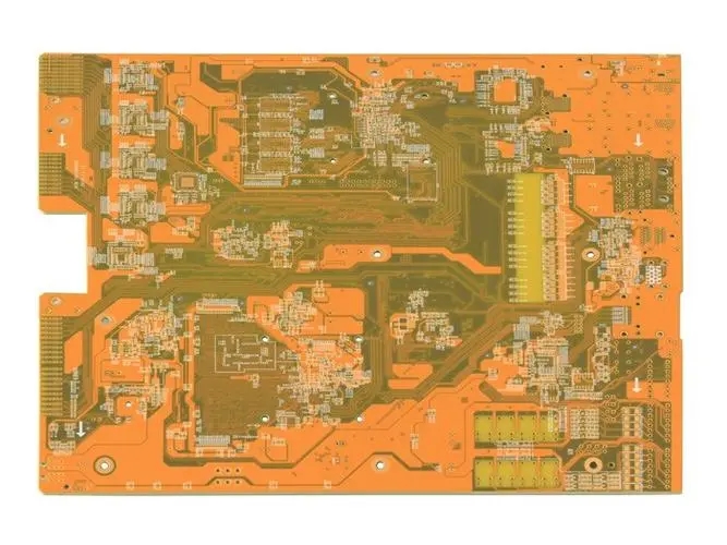
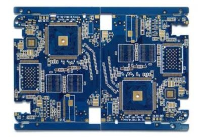
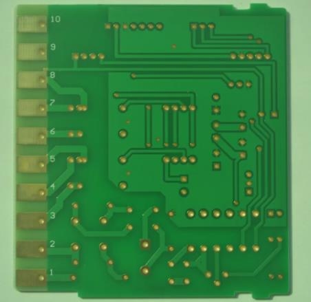
The Circuit board manufacturer and circuit board designer will explain how to strengthen BGA from the design end to prevent its solder joints from cracking.


Telegram
Gerberファイル、BOMファイル、および設計ファイルをアップロードするだけで、KINGFORDチームは24時間以内に完全な見積もりを提供します。