
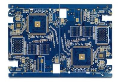
Kingfordは「高品質、短納期、小量の試作生産から量産まで」というお客様のニーズにお応えします

The Method of Improving PCB Design EffICiency by Software SIMulation
Software simulation
In the newly developed simulation software package, users can see the complete wiring design from the most popular PCB layout tools. The wiring review function will check various design principles of all boards, networks or traces. The software can import the routing data of the following routing tool providers: Altium, CADence, Mentor, OrCAD and Zuken. The software is jointly developed by experts from professional simulation software companies and well-known IT industry giants. The former provides interfaces with a variety of PCB routing tools, while the latter focuses on establishing and verifying expert systems for EMC/SI rules for decades. Over the years, the company's experts have studied many EMC design problems using flexible measurement technology, and finally established various effective design rules. The key design shall be checked according to these rules, and the results shall be verified by testing. Finally, different functions are combined to form a software tool that can identify the main sources of common electromagnetic disturbances.
This general-purpose software does not need EMC experts. It allows PCBA board designers to check whether the design conforms to EMC rules. Secondly, the software provides cabling designers with detaiLED descriptions and possible solutions to EM problems. The integrated browser can display the exact locations in the design that violate EMC rules. In fact, the main purpose of developing this software package is to enable users without relevant EMC knowledge background to accurately locate EMC problems earlier and easier in the design, so as to minimize the cost of measurement and redesign.
Rule based inspection
EMIssion or coupling is caused by violation of some geometric rules. For example, considering the path of current return, each signal has a preset path of signal path, but there are often loops in the power layer and ground plane. Loop current always chooses the path with the lowest resistance; At the same time, choose the path with the lowest impedance under high frequency conditions. This new software can determine which return path is discontinuous. For example, this path may be interrupted due to a detached plane. If the loop cannot follow the signal path geometrically, the loop current uses a different path. Depending on the size of the area around the loop current, an antenna may radiate or receive interference signals, leading to EMC compliance failure or possible design failure. This software tool identifies whether such discontinuous copper in the power supply layer is connected by one or more capacitors for high frequency (Figure 1). Those capacitors will form a path with low impedance to the loop current, thus avoiding unwanted loops.
Another rule is to search for networks that change the reference plane of the signal layer and the loop current. If the signal trace changes only from above to below the reference plane, the radiation generated is very SMAll. In this case, the loop current can continue to flow in the same plane. If the signal layer and the reference plane change at the same time, the return path must be guaranteed (as shown in Figure 2). When capacitors are used near vias, unwanted path and loop currents must be avoided. This software design rule must identify and allow the layer change in the porous area below the BGA, because the return current will not pass through the capacitor but will pass through the BGA. If this principle is violated, the vias where the layer changes will be highlighted by the software.
If the signal layer and the reference plane change at the same time. At higher signal frequencies, it is necessary to reduce the length of the external layer line, check the maximum allowable length of the cable, and point out the violations.
Another rule will check the maximum distance from the connecting pin of the isolated capacitor to the supply voltage. Because the effective radius of the DC isolating capacitor is very small, the distance allowed to connect to the decoupling pin cannot be exceeded. Otherwise, the capacitor is useless and can be ignored. Violation of this rule will be listed together with the distance to each capacitor. The last important rule is that the trace should not be too close to the edge of the reference plane layer. In this case, the line impedance will change and may cause the signal to reflect at the discontinuity of impedance.
With this software package, you can check specific rules, guide users through an error list, and then display the key areas of wiring. Changing the position of components at the early stage of the design stage can create a wiring path to prevent electromagnetic compatibility problems, without additional shielding or filters, thus saving valuable circuit board space and component costs.
conclusion
As the circuit board design becomes more and more complex and the EMC specification develops more and more strictly, it is necessary to seek solutions at the early stage of the design stage. Software simulation package, especially when it is used together with the effective interface of widely used cabling tools, is of great significance in the product development process.


Telegram
Gerberファイル、BOMファイル、および設計ファイルをアップロードするだけで、KINGFORDチームは24時間以内に完全な見積もりを提供します。