
Kingfordは「高品質、短納期、小量の試作生産から量産まで」というお客様のニーズにお応えします

Code for design of circuit board ----- Code for Design of ThICk Copper board
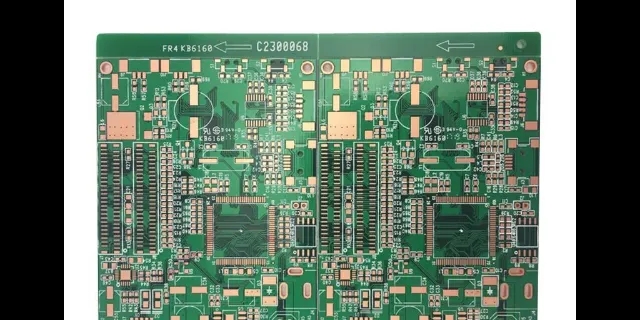
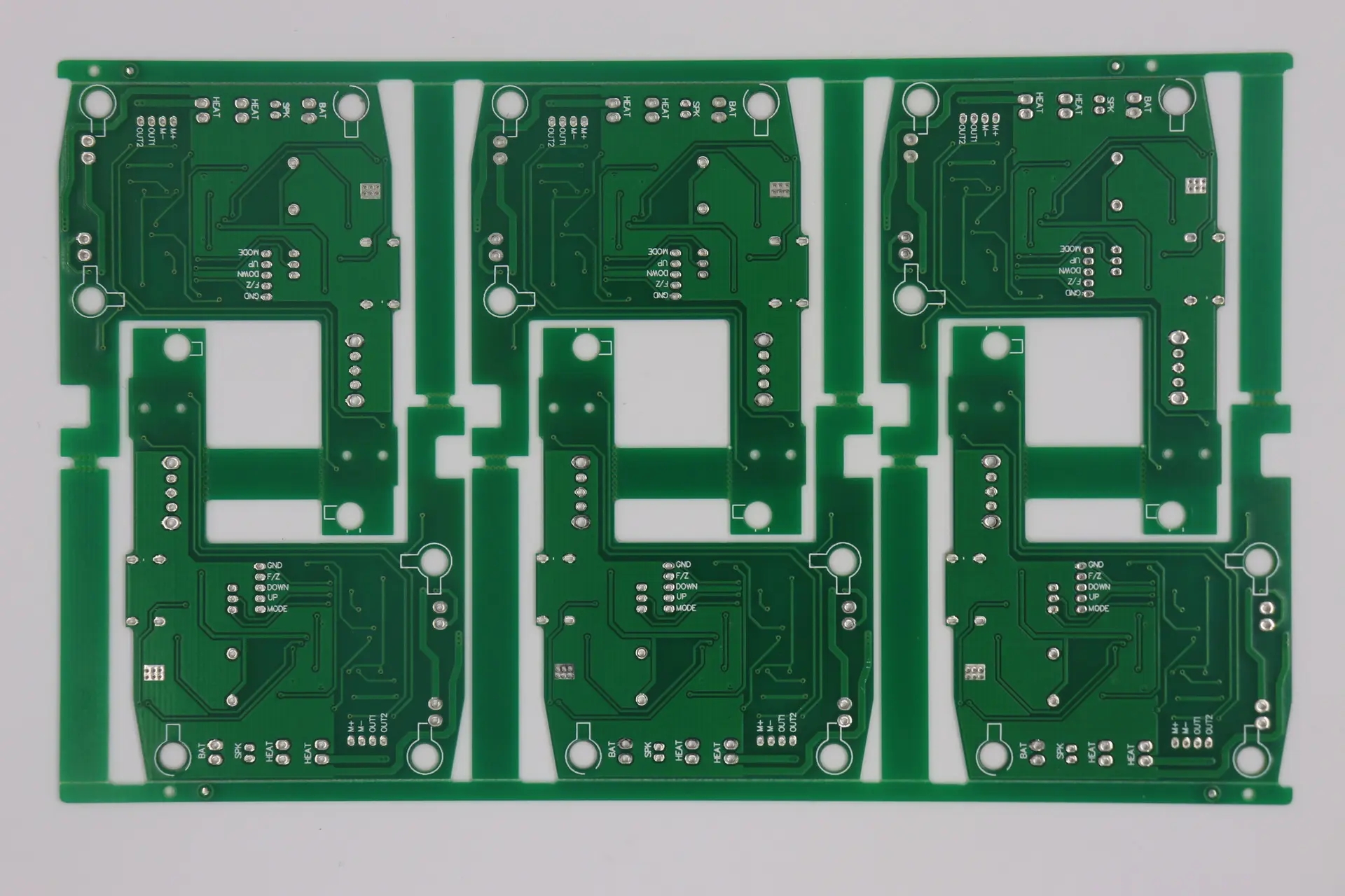
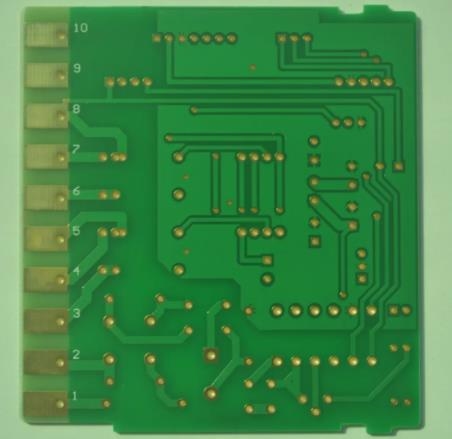
For PCB boards with a copper thickness of more than 2 ounces, due to the copper thickness, the circuit board design specification is different from that of general circuit boards. Therefore, the company specially specifies a document inspection specification for thick copper boards, so as to provide customers with better quality circuit boards.
1: Code for Wire Design of Circuit board Design
A: The minimum wire width of the circuit board shall not be less than 0.3mm;
B: The minimum distance between adjacent conductors in general shall not be less than 0.25mm
C: The distance between the copper foil around the fixing hole and the hole edge shall not be less than 0.4 mm; There should be no thin wire 1.5mm from the edge of the hole
E: Whether low density cabling design is considered
F: Whether the wires are laid according to the shortest route and whether there is no acute angle at the turning
G: Whether the junction between the wire and the bonding pad is smoothly processed into a slope
H: In the power circuit, the distance between adjacent conductors between hot and cold ground shall not be less than 6mm
1: The distance between the conductor and the edge of the printed board is generally not less than 3mm, and in particular not less than 1.5mm, but the wiring width must not be less than 1.5mm; Ground wire shall not be less than 0.5mm
2: Design specification for bonding pad of circuit Board Design
A: The distance between the bonding pad of the plug-in component and the edge of the printed board shall not be less than 7mm in general, and 3.5mm in special cases. The distance between the bonding pad of the mounting component and the edge shall not be less than 5mm; For the plate edge with process edge to be reserved, the distance from the solid and pad of plug-in components or mounting components to the plate edge shall not be less than 5mm
B: The connection (pad) spacing of IC with pin spacing of 1.78mm should not be less than 0.3mm
C: Whether the minimum diameter of the round pad meets the standard
D: Whether the bonding pad of components inserted after wave soldering is removed from the tin bath
E: No connection between pads or between pads and bare copper foil
F: Whether the bonding pad of the switching transformer and harmonic current suppressor is removed from the empty pin bonding pad to prevent incorrect insertion
G: Whether the filter inductance of AC input circuit, switch transformer, inverter transformer, high-power resistor, high-power damping or rectifier straddle diode (non plastic package), and the bonding pad of rectifier large electrolytic capacitor are reinforced with rivets
H: The number of rivet pads for multi pin component pads should generally not be less than 1/2 of the number of pins of the component
1: Whether the design requirements of rivet hole pad meet the standards; The rivet pad with a hole diameter of 1.8mm is 4.5mm. If it does not meet the requirements, 4.0mm pad shall be added with water drop tin for reinforcement. The rivet pad with a hole diameter of 2.4mm shall be 5.5mm. If it does not meet the requirements, 5.0mm pad shall be added with water drop tin for reinforcement
J: With the positioning hole of the printed board as the center, no rivet pad will be designed within the radius of 7 mm, and no rivet pad will be designed if the distance between adjacent holes is less than 6 mm
H: Whether the key components are reinforced with rivets, and whether the bonding pads of key components are coated with tin in the form of water drops
3: Thermal Design Code for Circuit Board Design
A: Whether the thermal element is far away from the radiator
B: Whether there are heat dissipation measures for high-power components
C: The distance between high-power heating device and large volume electrolytic capacitor shall be greater than 5mm
D: Whether the heat conduction facilities of the device are considered
E: Whether the fixing and position of radiator are proper
F: There should be a proper amount of heat dissipation holes under and around the corresponding printed board of the heating device, whose diameter is generally not more than 4mm
G: Large area copper foil is easy to expand due to heating, and the conductive layer must be provided with a conductive window in the area exceeding a circle with a diameter of 15mm
4: Layout design specification for circuit board design
A: Whether the production can be completed through the SIMplest assembly process
B: Whether the high-power devices are evenly distributed, whether the flow direction of heat dissipation is considered, and whether the board bearing strength
C: Whether fixing devices are added for high quality components
D: Whether insulation measures of components are considered
E: Whether the elements are arranged horizontally or vertically
F: The radiator must not touch the surrounding elements
G: Whether the cushion column position is evenly distributed
H: Whether there are nail bottom elements and flying wires
1: Whether the installation of heat sink conforms to the cooling flow direction, whether the existing heat sink is used as much as possible to reduce the possibility of making new heat sink
J: Whether the maximum PCB length is not more than 600mm and the width is not more than 360mm
K: Whether the cold ground installation fixing hole is equipped with grounding lug, and whether the grounding lug is sufficient
50: Whether there are more than three global MARK points on the copper foil surface of the board, and whether the increased positions meet the process requirements and affect the safety distance
M: Whether the arrangement of vertical electric plug elements can ensure that the outer edge distance between parts is more than 1mm
N: Whether there are solder pads and copper foils easy to tin on the edges of printed boards, which makes assembly difficult
O: Whether the fixing method is considered for the riser
P: Whether there is space for components fixed on the radiator to be disassembLED without disassembling the radiator
Q: Whether there are tall and dense components or sharp radiator corners around the row plug
R: Whether the placement position of input/output plug meets the convenience of connecting with other boards of the whole machine
S: Whether the patch element is placed perpendicular to the long side of the plate to avoid fracture or damage due to deformation
T: Whether the plug-in IC and chip IC are horizontally placed in the same direction as the wave soldering process, and whether the IC is designed with solder pad at the appropriate position during wave soldering to avoid continuous soldering of the furnace soldering pad
U: Whether to avoid shadow effect when placing all patch components
5: Whether there is positional interference between the screws fixing the components and the radiator and the components on the board
5: Welding design specification for circuit board design
A: Whether 3mm wide reserved support strip is reserved in the middle of PCB boards wider than 180mm or longer than 320mm for wave soldering
B: The reserved position of the support strip shall not be within the bending range of the component lead
C: For components that are not suitable for wave soldering due to structural limitations, it is necessary to add a tin bath at the position opposite to the wave peak direction, with a bath width of 0.7mm
D: The wave soldering direction shall be clearly marked on the upper and lower sides of the plate
E: Try not to arrange components with space size extending out of the board edge such as horizontal patch cord
F: The bending part of the electric plug element lead, the area around the triode, IC and strip pin pad shall be coated with a secondary solder mask
G: Large area of copper foil is easy to expand due to heating, so the conductive layer needs to open a conductive window or grid in the area exceeding a circle with a diameter of 15mm


Telegram
Gerberファイル、BOMファイル、および設計ファイルをアップロードするだけで、KINGFORDチームは24時間以内に完全な見積もりを提供します。